Micron’s Next-Gen HBM Pushes Memory Bandwidth Boundaries

Memory is one of the biggest bottlenecks in machine learning. In a turn of events, AI accelerators used to train machine-learning (ML) models in the data center and processors to execute them can only run as fast as they access data from memory. The problem? As these models get larger and larger, the chips require more memory to store them and as much memory bandwidth as possible to fetch data faster.
Micron is trying to overcome the memory bottleneck with a new generation of high-bandwidth memory (HBM) for the data centers and supercomputers being built specifically for AI—known as HBM3 Gen2.
Boasting a 2.5X generational leap in performance per watt, Micron said the 24-GB chip set “new records” in several metrics that are important to data centers, namely performance, capacity, and power efficiency.
Its latest HBM3 memory features faster signaling rates, up to 9.2 Gb/s per pin, giving it more than 1.2 Tb/s of memory bandwidth. The memory chip giant touted this as a 50% improvement over the base HBM3 chips from Samsung Electronics and SK Hynix. Further, the chips bring 50% more memory density to the table than the HBM3 Gen2—also called HBM3E—being rolled out by rivals.
The higher memory density and improvements in memory bandwidth help reduce how long it takes to train the most advanced large language models (LLM), which are emerging in everything from OpenAI’s ChatGPT to Google’s Bard, by more than 30%, said Micron.
Mass production of the HBM3 Gen2 memory is expected to begin by early 2024. Sampling is underway.
HBM Rides High for AI
HBM is a type of high-performance 3D memory that was designed to address the bandwidth limitations of DRAM and its inability to keep up with the performance and power efficiency of CPUs, GPUs, and other chips in the data center.
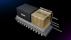
HBM is assembled out of several DRAM memory die stacked in three dimensions. It’s stitched together with microscopic interconnects called through silicon vias (TSVs) that run through them like elevators linking the floors of a building.
Featuring a smaller form factor than DRAM, HBM can be placed in closer proximity to CPUs, GPUs, and other chips. With a memory bus that measures 1,024 bits wide—up to 128X wider than DDR DRAM—HBM is frequently attached to the same silicon interposer or other advanced package as the processor or accelerator, shrinking the distance data needs to travel between them and reducing the power spent on data movement.
Even though it costs more than standard DRAM, HBM makes it possible for GPU, CPU, and other core components in the data center, such as FPGAs and AI accelerators, to access data faster than it can through a traditional CPU socket interface.
While not a cure-all for the challenges bearing down on the data center, HBM is increasingly playing a pivotal role in the AI boom. It’s becoming one of the core building blocks in AI accelerators in the data center, including NVIDIA’s H100. The data-center GPU, the gold standard in AI training and priced at more than $20,000 per unit, is bordered by 80 GB of HBM3 memory sporting 3.2 Tb/s of memory bandwidth.
That enables larger ML models to fit inside the package’s memory—the next best place to store the models after on-chip SRAM—reducing latency that can limit the performance of AI workloads.
HBM is also part of the plan for any company trying to compete with NVIDIA in the market for AI silicon. Driven largely by next-generation AI accelerator chips, global demand for HBM is estimated to grow by almost 60% annually in 2023, totaling 290 million GB of memory, with another 30% rise in 2024, according to market research firm TrendForce. HBM3 is on track to become mainstream next year.
AMD is leveraging it in even larger quantities in its future AI accelerator chip for the data-center market, the MI300X. The GPU is equipped with up to eight HBM3 cubes, totaling up to 192 GB of memory.
The vast amount of memory means that a single CDNA3-based AI accelerator can run ML models containing up to 80 billion parameters, which the company touted as a record for a single GPU.
More Dimensions, More Memory
As the latest machine-learning models continue to expand—with the most advanced versions measuring tens of billions to trillions of parameters—AI chips in data centers are in dire need of more memory bandwidth.
Micron, which ignored the first generation of HBM3 to focus instead on the more advanced HBM3 Gen2 technology, is betting its high-bandwidth memory chips will help it secure a larger role in the AI boom.
The HBM3 Gen2 memory is based on Micron’s latest 1β DRAM process technology, which gives it the ability to assemble up to eight separate slabs of silicon into a cube-shaped memory chip that contains up to 24 GB of capacity. The company said its new process technology delivers 50% more density at a given stack height and that it plans to start sampling its 12-die stack with 36 GB capacity in the first quarter of 2024.
In addition, its HBM3 Gen2 memory chips feature data rates as fast as 9.2 Gb/s, more than 40% faster than the maximum 6.4-Gb/s speed of the base HBM3 standard.
The performance-to-power ratio and pin speeds of Micron’s HBM help manage the high power demands of data centers, which are being expanded rapidly across the industry for the purposes of AI.
Improved power efficiency is possible thanks to several innovations. Importantly, Micron said it doubled the number of TSVs, enabling more parallel data transfers, which pays dividends in bandwidth and power efficiency while keeping a limit on latency. The paths that data travels through the HBM3 memory chip are more efficient than in its predecessors, too. The company also cited a 5X increase in metal density, helping to reduce thermal impedance in the module.
The performance-per-watt of the HBM3 Gen2 chip, which also has the advantage of being drop-in compatible with existing HBM3 memory chips on the market, is driving cost savings for AI data centers. For an installation of 10 million GPUs, Micron estimated that every 5 W of power savings per HBM attached to it will save operational expenses of up to $550 million in a five-year span.
Micron is also partnering with TSMC to improve the integration of its HBM3 Gen2 memory into AI and other high-performance computing (HPC) chips using TSMC’s 2.5D and 3D packaging tech.
About the Author

James Morra
Senior Editor
James Morra is the senior editor for Electronic Design, covering the semiconductor industry and new technology trends, with a focus on power electronics and power management. He also reports on the business behind electrical engineering, including the electronics supply chain. He joined Electronic Design in 2015 and is based in Chicago, Illinois.
Comment About the Article
To join the conversation, and become an exclusive member of Electronic Design, create an account today!

Leaders relevant to this article: