3D NAND Flash Memory Continues Its Climb
Check out our coverage of the 2023 Flash Memory Summit.
3D NAND chips are the skyscrapers of the semiconductor industry, linking together layers of flash memory with short vertical interconnects that act like elevator shafts connecting the floors of a high-rise building.
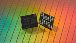
But as the recent boom in artificial intelligence (AI) drives up the demand for memory, semiconductor companies are racing to control the skyline. SK Hynix, the world’s second-largest memory chipmaker, is trying to pull ahead with a new generation of its "4D NAND" assembled out of 321 layers of NAND flash. Prototypes of the technology were on display at the Flash Memory Summit (FMS) in Santa Clara, Calif.
With mass production more than a year and a half out at this point, SK Hynix is still in the early stages of development. But the announcement signals that it’s progressing on the path to the world’s first 3D NAND with more than 300 layers, and that the company intends to leap out ahead of its rivals in the memory wars. Improvements in density make it possible to store more data in a given space, driving down costs. Increasing density tends to yield better power efficiency and higher bandwidth, too.
A year ago, Micron said it had begun mass production of its most advanced 3D NAND chips composed of 232 layers, jumping ahead of SK Hynix and Samsung Electronics in supplying 3D NAND with more than 200 layers.
It All Stacks Up
While the future of flash memory requires improvements in memory controllers used to read, write, and erase data to storage drives and firmware to run on top of them, memory innovations are at the heart of it all. Stacking memory in three dimensions is a serious engineering challenge. But it’s important to increase the amount of data that can be stored in every square millimeter of silicon in a 3D NAND chip.
SK Hynix refers to its NAND flash technology as “4D NAND,” since it stacks the memory cells at the heart of its memory chips on top of the CMOS logic used to coordinate the reading and writing of data fast and efficiently. In its latest 238-layer 3D NAND, the company also applies “string stacking” to unite a pair of 119-layer slabs of memory cells based on its “charge-trap flash” technology on a die.
Though it refused to reveal any of the technology behind the 300-layer NAND flash memory, the company said it’s applying what it learned from the current 238-layer 3D NAND to address the stacking limitations.
Whatever the improvements, they translate to 1 Tb of capacity in a single chip using a three-level-cell (TLC) construction that fits three units of data per cell. That doubles the 512 Gb of storage per die in its current generation of 238-layer 3D NAND, which entered mass production this year. Higher density translates to more memory capacity per die, which ultimately pays dividends in everything from smartphones and other consumer electronics to data centers.
The new 3D NAND chips are projected to enter mass production in the first half of 2025.
Check out more coverage of the 2023 Flash Memory Summit.
About the Author

James Morra
Senior Editor
James Morra is the senior editor for Electronic Design, covering the semiconductor industry and new technology trends, with a focus on power electronics and power management. He also reports on the business behind electrical engineering, including the electronics supply chain. He joined Electronic Design in 2015 and is based in Chicago, Illinois.
Comment About the Article
To join the conversation, and become an exclusive member of Electronic Design, create an account today!

Leaders relevant to this article: