Timing Decisions 102: Optimize Your Clock Tree

This article is part of the TechXchange: Oscillations, Timing and Synchronization.
Members can download this article in PDF format.
What you’ll learn:
- The importance of timing requirements and jitter budgets for FPGAs, ASICs, and SoCs.
- How to utilize the information portrayed in a clock tree to choose the most well-suited clock generator for your application.
- The impact jitter can have on your timing performance.
In our last article, we provided an overview of the design considerations when developing a reliable timing system. Notably, this revolved around the crucial decision made between selecting crystal oscillators and clock generators. Now we’ll dig into this discussion deeper, exploring clock trees, jitter budgets, and how to select a clock generator for a given design.
Modern applications are built around high-bandwidth, multicore processors, and field-programmable gate arrays (FPGAs), which often have stringent timing requirements and jitter budgets. Given the frequency diversity of these applications, the choice between an oscillator and an integrated clock becomes much more straightforward.
Oscillators and Clock Generators
An oscillator is able to generate one reference frequency for a single device. If an application has modest timing requirements, one or two oscillators can be used in the design. For applications that require a greater number of frequencies or clocks, it may be prohibitive to use crystal oscillators due to cost, PCB layout complexity, or reliability, since each oscillator represents a potential point of failure in the system.
A better approach for these applications is to use a clock device that consolidates multiple oscillators into a solid-state integrated-circuit (IC) solution. This simplified solution offers additional benefits for the designer, including improved reliability, the ability to switch clock frequencies if system requirements change, simplified procurement, and more. Thus, integrated clock generators emerge as the primary solution for more complex systems and applications.
Knowing the timing requirements and jitter budgets for FPGAs, ASICs, and systems-on-chip (SoCs) is what enables us to make the initial decision between an oscillator or a clock generator. Beyond that, it allows us to take it a step further and decide which clock generator is right for a given application. To take this next step, we need a way to define this information. Enter the clock tree and its jitter budget.
What’s a Clock Tree?
The clock tree, a hardware design’s clock-distribution network, includes the clocking circuitry and devices needed for frequency synthesis and clock distribution between the clock source and each individual IC. Typically, a single reference clock will drive multiple clock paths, much in the same way a tree has multiple branches connected to a common trunk.
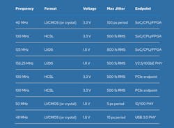
To optimize the clock tree for a given application, hardware designers need to understand the requirements associated with each individual IC. Each FPGA, ASIC, and SoC datasheet typically lists the frequency, clock signal format, voltage level, and applicable maximum jitter associated with each reference clock. The same information may be similarly provided in a reference block diagram in the SoC datasheet.
Formatting the collected information into a single reference table (Fig. 1) is an essential step to ensure all system requirements are captured.
The next step in the process is to select the timing ICs that provide clock generation and clock distribution. These devices must meet the design’s specific needs and provide sufficient margin to critical jitter budgets to help ensure first-pass success.
The detailed jitter requirements from the clock tree opens the door to a larger conversation around jitter and the budget for the entire system.
Defining the Clock-Tree Jitter Budget
Jitter is the key figure of merit for timing performance, and more specifically, the variation in the accuracy of a clock period. In high-speed communications systems, it’s critical to manage jitter carefully to prevent degradation in the data transmission’s bit-error rate. Physical-layer transceivers in FPGA/ASIC/SoCs, used to carry serial data between two devices, will typically specify the maximum allowable jitter the transceiver reference clock can tolerate before it violates system performance. Maximum jitter is a specification that comprehensively includes variation over process, voltage, temperature, and other operating conditions, and includes support for any applicable industry standards.
A common rule of thumb is to optimize the clock-tree design for the most jitter-sensitive reference clocks first by selecting clock generators that generate these frequencies using a high-performance phase-locked loop (PLL) and integer dividers. It’s important to compare the clock generator’s maximum jitter specification versus the reference clock requirement to ensure there is sufficient safety margin.
Avoid clocking devices that specify typical jitter and don’t guarantee maximum jitter since they may suffer from higher variability over process, voltage, temperature, and/or frequency configuration. Using a high-performance PLL with integer dividers ensures the system’s most critical clocks have excellent phase noise and low spurious content.
Unrelated and Multiple Single Frequencies
Second, the system may require frequencies that are entirely unrelated to each other. After deciding which clocking device will be used to generate the most jitter-sensitive clocks, the next step is to determine how to generate the rest of the system frequencies.
Today, programmable clock generators are available from multiple suppliers that support integrated fractional dividers, which can be used to synthesize unrelated clock frequencies. Fractional dividers provide frequency flexibility, but the tradeoff is higher jitter generation. The ideal selection is a clock generator device that can synthesize the most jitter-sensitive integer clocks while simultaneously generating fractional, unrelated clocks with sufficient margin to FPGA/ASIC/SoC reference clock requirements.
Some systems require multiple copies of a single frequency. In these applications, a clock buffer can be used to provide the distribution of a clock from an oscillator or clock generator IC.
For clock buffers, the key figure of merit is additive jitter, which typically impacts the wideband noise of the clock. Additive jitter represents the amount of jitter, or clock noise, that’s added to a clock signal as it’s distributed. If a clock buffer is used to fan out a clock from a clock generator IC, it’s critically important to ensure the combined clock signal provides sufficient margin to the downstream FPGA/ASIC/SoC’s reference clock requirement.
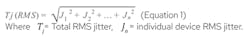
Clock trees typically use clock generators or oscillators for frequency synthesis, and clock buffers as follow-on devices for clock distribution. A root-sum-square (RSS) equation (Fig. 2) can be used to estimate the total jitter through the frequency synthesis and clock-distribution devices. This estimate can then be compared against the FPGA/SoC’s maximum jitter specification to ensure sufficient headroom is available.
Considering the Timing Design
Understanding the clock tree itself, in addition to the total clock-tree jitter, gives a system designer the ability to allocate the timing system accordingly. It also helps ensure the frequency synthesis and clock-distribution devices have sufficient margin versus maximum system-level jitter requirements.
Outside of this, certain aspects of hardware design are subject to change prior to completion, and these factors may impact the clock tree’s frequencies and signal formats. Changes in the design due to component selection or architectural changes to the physical-layer or control plane design may dictate the need for clocks with different frequencies or signal formats.
In addition, FPGAs are highly reconfigurable. If the required FPGA feature set changes considerably based on market and application requirements, it may necessitate a hardware change that impacts the clock tree. For these reasons, it’s advantageous to use a device capable of supporting any frequency synthesis and built-in signal format translation.
Clock generators that can generate any frequency on any output, while simultaneously offering signal format translation, are often the best choice. One key function that a clock generator can’t provide is jitter cleaning. When jitter cleaning is needed within the timing system, a jitter attenuator can be used in lieu of a clock generator within the clock tree. Vendors now offer solutions that provide clock generation and jitter attenuation in a common PCB footprint, easing the transition if a jitter attenuator is required.
As high-speed applications continue to push data bandwidth limits skyward, applications require an increasingly diverse mix of frequencies with ever-tighter jitter budgets. Designing a reliable clock tree is becoming more crucial than ever. By considering the different requirements tied to the clock tree as a whole, it makes it possible to choose the best solution for each application.
Read more articles in the TechXchange: Oscillations, Timing and Synchronization.
About the Author
James Wilson
VP & General Manager, Skyworks
James Wilson is the Vice President and General Manager of timing products at Skyworks Solutions Inc. In this role, James manages the company’s overall timing business and directing product strategy, new product initiatives, product management, software development, and marketing initiatives for Skyworks’ extensive timing portfolio. James has extensive experience in timing and communications, with a career that spans over 22 years across different leadership roles at semiconductor and technology companies including Silicon Labs, General Bandwidth, and Freescale.
Comment About the Article
To join the conversation, and become an exclusive member of Electronic Design, create an account today!

Leaders relevant to this article: