NVIDIA RTX 3080: Real-Time Ray Tracing on a Chip
This article is part of the Electronics History series: The Graphics Chip Chronicles.
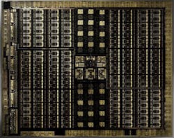
In early 2018, NVIDIA showcased hardware-accelerated real-time ray tracing using its DGX system and the DXR API. The $50,000 DGX contained four NVLink 4-Way interconnected NVIDIA Tesla V100 add-in boards (AIBs). Each AIB featured a 5,120-shader Volta GPU running at 1.46 GHz with 16 GB of HMB2 local memory and was capable of 7 TFLOPS double-precision, for a total of 40,960 shaders and 128 GB of memory.
The cluster of AI accelerators was paired with a 2.2-Hz, 20-core Intel Xeon E5-2698 processor equipped with 256-GB DDR4 that could produce 800 GFLOPS, which in total pumped out a theoretical compute capability of 28.8 TFLOPS. But given that it was necessary to run the workload on a small supercomputer, I predicted that it would take more than half a decade to bring real-time ray tracing inside a single GPU.
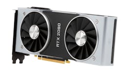
Upon the introduction of the “Turing” GPU architecture in late 2018, the company signaled it was ready to bring real-time ray-tracing technology to consumers everywhere. NVIDIA surprised everyone, showing off real-time ray tracing running for the first time on a single chip—the RTX Turing TU102 GPU, placed in the GeForce RTX 2080 AIB. The industry had a new acronym—RTRT—for real-time ray tracing. NVIDIA also introduced its Quadro RTX AIBs at Siggraph at the same time.
What is Real-Time Ray Tracing?
Ray tracing is a complex process of generating light rays that illuminate a visible scene combined with the bounces and reflections of those visible rays. Millions, if not billions, of rays are generated, and their luminosity and color must be calculated for every instance of interaction they experience. It’s a horrendous calculation workload that’s aggravated by resolution because the number of visible pixels goes up as the product of X times Y.
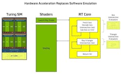
The RTX AIBs based on the Turing GPU featured fixed-function “RT” inference cores designed to accelerate the operations needed to simulate rays, such as bounding volume hierarchy traversal. NVIDIA also introduced DLSS, leveraging AI to improve gaming performance.
Turing GPUs incorporated tensor cores for matrix math processing. Texture-Space Shading allowed for efficient caching and sampling of shading results. The Turing architecture laid the foundation for dedicated ray tracing and tensor engines, full mesh shading capabilities, and advances in real-time rendering.
When it formally introduced the GeForce RTX 20 series AIBs a month after unveiling its Turing GPU, NVIDIA promoted DLSS as a prominent feature. However, initially, its application was limited to a few video games, such as Battlefield V and Metro Exodus. This was because the algorithm required individual training for each game, and the outcomes were generally not as impressive as basic resolution upscaling.
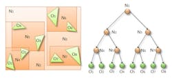
In the context of geometric objects, a bounding volume hierarchy (BVH) is a tree structure utilized to organize and categorize objects. The objects themselves serve as the nodes or leaves of the tree, and they’re enveloped by bounding volumes.
Those nodes are further organized into smaller sets and enclosed within larger bounding volumes. This recursive grouping process continues, with the nested nodes being enclosed within increasingly larger bounding volumes, ultimately forming a tree-like structure where a single bounding volume encompasses the entire hierarchy. BVHs find application in collision detection (inference detection) in ray tracing.
Solving the ray-tracing algorithm was step one. The other, maybe larger, problem was managing the screen resolution.
Turing: The First Consumer AI Processor?
In 2017, NVIDIA was enjoying the take up of GPUs in the data center for compute acceleration. At the same time, AI training was getting into full swing, and as fate would have it, AI training was (is) an ideal candidate for parallel processing—the GPU’s major strength.
However, AI needed another type of recursive processing that involved matrix math. Matrix can be done on a GPU, but it’s not the most efficient engine. Other approaches tried by other firms were digital signal processors (DSPs) and dedicated matrix-math processors constructed in field-programmable gate arrays (FPGAs). DSPs were—and are—used successfully in mobile devices such as smartphones, and Qualcomm is a leader in the area. FPGAs are programmable and functionally effective but not fast.
A new, dedicated matrix-math processor was needed. Google was one of the first to offer such a device, naming it a tensor processor unit, or TPU. In mathematics, a tensor is an algebraic object that describes a multilinear relationship between sets of algebraic objects related to a vector space. The straightforward way to think about it is that a tensor processor does 3D processing in real-time.
The NVIDIA Turing GPU being employed in the RTX 2080 AIB (and Quadro RTX AIB) was equipped with custom math engines—inference engines for ray tracing and tensor engines for matrix math.
Another feature of the new GPU was Deep Learning Super-Sampling (DLSS). NVIDIA claimed the tensor cores in the GPU could be used to improve gaming performance using DLSS. DLSS leverages a deep neural network to extract multidimensional features of the rendered scene and intelligently combine details from multiple frames to construct a high-quality final image. Thus, Turing GPUs can use half the samples for rendering and AI to fill in the information to create the final image.
The result, said NVIDIA, is an image with similar quality as traditional rendering used in many of today’s latest games but with higher performance. NVIDIA said DLSS was an easy integration for developers, and at the time, developers announced 25 games would have DLSS support.
Therefore, it’s not a stretch to call the Turing GPU the first general-purpose consumer AI processor. On top of the thousands of SIMD processors, video/display/audio processors, raster operation processors, memory managers, and I/O processors, the Turing GPU gained two new processing blocks: the ray-tracing, or RT, and Tensor cores.
The Turing architecture introduced important enhancements to the core execution data paths. Previous shader workloads consisted of a combination of floating-point (FP) arithmetic instructions, such as floating add (FADD) or floating multiply (FMAD), along with simpler instructions like integer adds for addressing and data retrieval, floating-point compares, or min/max for result processing, and more.
In prior shader architectures, the floating-point math data path remains inactive whenever one of those non-FP-math instructions is executed. Turing addressed that limitation by incorporating a second parallel execution unit alongside each CUDA core.
Within the new architecture, the primary enablers for Turing’s improvement in graphics performance were a new GPU processor (streaming multiprocessor, or SM) architecture with improved shader execution efficiency and a new memory system architecture that includes support for the latest GDDR6 memory technology. As NVIDIA explained, the Turing SM is partitioned into four processing blocks, each with 16 FP32 cores, 16 INT32 cores, two Tensor cores, one warp scheduler, and one dispatch unit.
In parallel with Turing’s development, Microsoft announced both the DirectML for AI and DirectX Raytracing (DXR) APIs in early 2018.
The Turing GPU was full of superlative numbers, equipped with 18.6 billion transistors (fabricated on TSMC’s 12-nm FinFET process node) that fit into a silicon area of 754 mm2—a new high on both fronts. In terms of performance, it pumped out 14.2 TFLOPS of peak single precision (FP32) performance, and NVIDIA touted several new metrics of GPU performance: 113.8 Tensor TFLOPS and 10 Giga Rays/s. The tradeoff is that it was a heavy user of power, consuming up to 280 W.
Turing packs 4,608 shaders (or as the company calls them, CUDA cores) capable of mesh shading. Mesh shading advanced geometry processing architecture by offering a new shader model for the vertex, tessellation, and geometry shading stages of the graphics pipeline, supporting more flexible and efficient approaches for the computation of geometry.
New GPU, New Graphics Capabilities
Another feature introduced with the Turing architecture was variable rate shading (VRS). VRS offers dynamic control over the frequency of shading in graphics rendering. Developers can adjust the shading rate, ranging from once per 16 pixels to eight times per pixel. VRS enables more efficient shading by reducing unnecessary work in areas of the screen, where full-resolution shading would not visibly enhance image quality.
Various categories of VRS-based algorithms have already been identified, including Content Adaptive Shading (which adjusts shading based on content level of detail), Motion Adaptive Shading (which varies shading based on the rate of content motion), and Foveated Rendering (which considers lens resolution and eye position, particularly in virtual reality).
Texture-Space Shading was yet another new development in the Turing architecture. Objects are shaded in a private coordinate space (a texture space) that’s saved to memory, and pixel shaders sample from that space rather than evaluate results directly. With the ability to cache shading results in memory and reuse/resample them, developers can eliminate duplicate shading work or use different sampling approaches that improve quality.
Turing was the foundation of a new generation of GPUs with dedicated ray tracing and tensor engines as well as full mesh-shading capabilities. NVIDIA paid for being first, and it was forced to encourage and support game developers to embrace the new rendering approach. Most of them welcomed it, but game development takes time, so major titles didn’t show up for a year or more.
AMD held back on implementing RT acceleration. However, when Intel entered the market with the launch of its Xe GPUs in September 2020, AMD offered it and its XLSS scaling capability. The company launched its first hardware RT accelerated GPU, the Radeon RX 6000, a month after Intel. By then, NVIDIA was on its second generation of real-time ray-tracing GPUs and preparing its third.
By mid-2023, NVIDIA had become the undisputed leader in real-time ray tracing. It was shipping DLSS 3.0, which improved the performance of the feature, allowing for 4K RTRT at respectable frame rates.
Read more articles in the Electronics History series: The Graphics Chip Chronicles.
About the Author

Jon Peddie
President
Dr. Jon Peddie heads up Tiburon, Calif.-based Jon Peddie Research. Peddie lectures at numerous conferences on topics pertaining to graphics technology and the emerging trends in digital media technology. He is the former president of Siggraph Pioneers, and is also the author of several books. Peddie was recently honored by the CAD Society with a lifetime achievement award. Peddie is a senior and lifetime member of IEEE (joined in 1963), and a former chair of the IEEE Super Computer Committee. Contact him at [email protected].
Comment About the Article
To join the conversation, and become an exclusive member of Electronic Design, create an account today!

Leaders relevant to this article: