Processing-in-Memory Accelerates AI

There are a host of hardware accelerators for various machine-learning ML models. To wit, Renesas has come up with a ternary SRAM-based system to accelerate convolutional-neural-network (CNN) computations. The CNN is a machine-learning class of deep-neural-network (DNN) models.
One of the challenges with ML is moving around input and output data as well as the weights involved in the calculations. Various approaches have been used to optimize data movement. For instance, Flex Logix’s NMAX keeps weights in local memory.
The ternary approach uses two single-bit memory cells to encode 1.5 bits of information as a -1, 0, or 1 (Fig. 1). The Processing-in-Memory (PIM) method takes advantage of the ternary values.
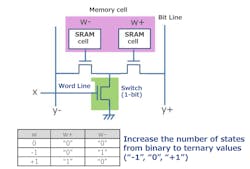
1. Renesas’ hardware can take advantage of a ternary memory cell that stores a value of -1, 0, or 1.
The basic ternary storage can be combined into multibit solutions. Blocks can be combined for different accuracies, allowing users to optimize the balance between accuracy and power consumption (Fig. 2).
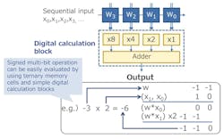
2. The hardware can combine ternary calculations into multibit operations.
Conventional memories read the contents using analog-to-digital converters (ADCs). This is a robust approach, but it requires space for the ADC and power. Renesas combined a 1-bit sense amplifier comparator with replica cells in which the current can be controlled flexibly to develop a high-precision memory data-readout circuit (Fig. 3). A “zero-detector” was developed to stop operation of the comparators when detecting the state that MAC result is equal to zero.
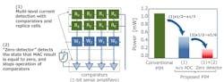
3. A “zero-detector” was developed to stop operation of the comparators when detecting the state that the MAC result is equal to zero.
This strategy takes advantage of the fact that the number of nodes (neurons) activated by neural-network operation is very small, about 1%, and it achieves even lower power operation by stopping operation of the readout circuits for nodes (neurons) that aren’t activated. As a result, power is significantly reduced while maintaining accuracy.
One downside of not using ADCs is that the storage isn’t as robust. Part of the issue stems from process variations during chip manufacturing. Renesas implemented multiple SRAM calculation blocks that have minimal manufacturing variations to address calculation errors due to manufacturing variations (Fig. 4). Normally, only a small number of all nodes will be activated. Nodes are allocated selectively to SRAM calculation circuit blocks that have minimal manufacturing process variations to perform the calculations. This allows calculation errors to be reduced to a level where they can be essentially ignored.
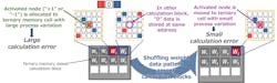
4. Multiple SRAM calculation blocks with minimal manufacturing variations are implemented to address calculation errors due to such variations.
Renesas engineers created a chip to demonstrate the ternary PIM approach (Fig. 5). The 12-nm technology chip contains four clusters, each containing the PIM and logic along with conventional SRAM storage. Each cluster can operate independently; thus, the system is able to manage up to four CNN models at one time. The chip can handle up to 128 CNN layers. PIM storage is 4.74 Mb and the SRAM stores 12.58 Mb. The 1-W chip can deliver 8.8 TOPS.
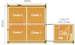
5. Renesas engineers created a chip to demonstrate the ternary PIM approach with four clusters. Each cluster can operate on a different ML model.
The chip has been used to execute a number of models, including one that recognizes handwritten characters. It maintained a recognition accuracy of over 99%. The chip is only a prototype, but it highlights how different approaches to ML acceleration can deliver higher performance while lowering power requirements.

About the Author

William G. Wong
Senior Content Director - Electronic Design and Microwaves & RF
I am Editor of Electronic Design focusing on embedded, software, and systems. As Senior Content Director, I also manage Microwaves & RF and I work with a great team of editors to provide engineers, programmers, developers and technical managers with interesting and useful articles and videos on a regular basis. Check out our free newsletters to see the latest content.
You can send press releases for new products for possible coverage on the website. I am also interested in receiving contributed articles for publishing on our website. Use our template and send to me along with a signed release form.
Check out my blog, AltEmbedded on Electronic Design, as well as his latest articles on this site that are listed below.
You can visit my social media via these links:
- AltEmbedded on Electronic Design
- Bill Wong on Facebook
- @AltEmbedded on Twitter
- Bill Wong on LinkedIn
I earned a Bachelor of Electrical Engineering at the Georgia Institute of Technology and a Masters in Computer Science from Rutgers University. I still do a bit of programming using everything from C and C++ to Rust and Ada/SPARK. I do a bit of PHP programming for Drupal websites. I have posted a few Drupal modules.
I still get a hand on software and electronic hardware. Some of this can be found on our Kit Close-Up video series. You can also see me on many of our TechXchange Talk videos. I am interested in a range of projects from robotics to artificial intelligence.
Comment About the Article
To join the conversation, and become an exclusive member of Electronic Design, create an account today!

Leaders relevant to this article: