Graphics Bus Wars: The Legacy of ISA, AGP, and PCI
What you’ll learn:
- A brief timeline of PC graphics bus interfaces.
- The history of the Peripheral Component Interconnect (PCI) bus.
- The status of the current industry-standard PCI Express (PCIe) bus.
Prior to the PC era, early microcomputers commonly used the S-100 bus—also known as the Altair bus—introduced in 1974 with the Altair 8800 microcomputer, developed by MITS (Micro Instrumentation and Telemetry Systems). It was named “S-100” after the 100-pin connector employed for expansion cards.
The pin layout for the S-100 bus was originally arranged by an unidentified engineer contracted by MITS. The layout was completed quickly and somewhat haphazardly, resulting in a pin configuration that lacked structure and wasn’t optimized for electrical noise resistance.
The pins were placed on both sides of the board in a way that minimized the number of plated through-holes while routing all 8080 signals to the bus. This design preceded the availability of modern computer-aided design (CAD) tools, which now enable much more efficient and optimized PCB layouts.
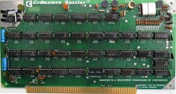
In 1976, Cromemco introduced the Dazzler, a graphics card for S-100 bus computers and the first color graphics card for microcomputers. It led to a series of advanced graphics products from the company, which by 1984 were used by 80% of U.S. television stations to display weather, news, and sports graphics.
From the S-100 to the ISA Bus
The S-100 bus—with its 8-bit data path and 16-bit address path—gained significant traction in the 1970s and early 1980s, eventually becoming the American National Standard IEEE Std 696–1983. However, IBM chose not to adopt it, instead developing its own expansion bus for the IBM PC.
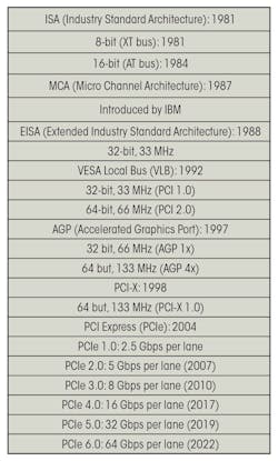
IBM designed its system with slots into which graphics and other peripheral boards could be plugged for power and communication with the CPU and system memory. When the IBM PC was introduced in 1981, it introduced the Industry Standard Architecture (ISA) card slot for expansion. At that time, a circuit board was needed to drive modems, displays, audio, and even hard disks. Today, all of these functions are typically integrated into a chipset.
From the ISA to the EISA Bus
The original ISA bus was 8 bits wide. When IBM introduced the PC/AT, it extended it to 16 bits and almost doubled the speed to 8 MHz—it became known as the AT bus. Over the following years, IBM introduced several proprietary bus designs, including the XT, which launched in 1983; the Micro Channel Architecture (MCA), which was introduced with the PS2 series in 1987; and, finally, the EISA, a 32-bit backward-compatible design introduced in 1988.
Although often associated with IBM, the Extended Industry Standard Architecture (EISA) wasn’t developed by the company. Instead, it was introduced by a consortium of nine IBM competitors—AST Research, Compaq, Epson, Hewlett-Packard, NEC, Olivetti, Tandy, Wyse Technology, and Zenith Data Systems—as a direct response to IBM’s proprietary MCA.
ELSA, a pioneering graphics board company based in Aachen, Germany, developed dual-interface boards compatible with both ISA and EISA sockets to address compatibility concerns with IBM’s PS/2 systems.
The VL Bus: Enter VESA
For many clone PC suppliers focused on low-cost systems, EISA was too expensive, largely due to IBM’s licensing fees. This led to the development of a private bus in 1992, branded by the Video Electronics Standards Association (VESA) as the VL (short for VESA Local) bus.
This led to a period of instability in the PC industry from 1986 to 1992, marked by competing bus standards with no physical or interoperability compatibility, and specifications that were too flexible, allowing for modifications. The widespread incompatibility led to frequent system crashes, with graphics boards having only a 50% chance of functioning across different computers.
But the “bus wars” were far from over.
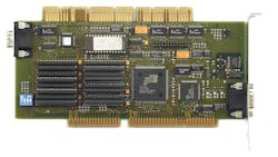
PCI: The Peripheral Component Interconnect Bus
In the late 1980s, Intel began designing a more advanced bus system in response to the growing market demand for a higher-bandwidth add-in board (AIB) interface. The result was the Peripheral Component Interconnect (PCI) bus, introduced in 1992 as a proposed industry standard.
As the predecessor to today’s ubiquitous PCI Express (PCIe) standard, PCI gained widespread adoption. In 1992, the PCI Special Interest Group (PCI-SIG) was formed to oversee its development and promotion.
One of the main advantages of the PCI bus was its improved interrupt request (IRQ) sharing, which helped eliminate the conflicts that plagued ISA-based systems. The new interface also introduced a more standardized approach to bus mastering, enabling devices to directly access system memory without relying solely on the CPU. PCI was created to replace the aging VL bus and older legacy approaches.

By 1995, PCI had become the dominant bus standard, effectively replacing VL, MCA, EISA, and other contenders within a year, bringing peace at last to PC land. However, the stability lasted a relatively short period of time: The PCI bus was introduced in 1993, and it succeeded the VL bus, which had been introduced a year before. But, in 1996, PCI began to be superseded by AGP for graphics applications.
AGP: The Accelerated Graphics Port
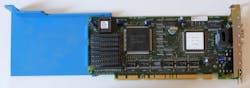
PCI was overtaken by the Accelerated Graphics Port (AGP) in 1997. It was designed specifically to meet the increasing need for speed in 3D graphics, which were becoming more common in consumer PCs. The AGP technology improved on the PCI bus by offering a direct connection between the graphics card and the motherboard chipset. It also allowed for direct access to system memory for texture storage, which is important for texture mapping in 3D graphics.
AGP provided higher bandwidth compared to PCI, initially starting at 266 MB/s for AGP 1x and eventually reaching 2.1 GB/s with AGP 8x. The first AGP boards and motherboards were introduced in mid-1997, and the standard was updated multiple times during its lifespan.
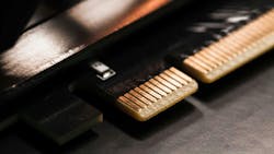
PCI Express: The New Standard for Connectivity
PCI Express (PCIe) was first introduced in 2003, with the specification finalized in July of that year. It began appearing inside consumer PCs in 2004.
Developed primarily by Intel, PCIe replaced PCI and AGP by introducing a radically different architecture: Instead of a shared parallel bus, PCIe used serial point-to-point links. This new approach led to much higher bandwidth and scalability.
The initial PCIe 1.0 specification offered 250 MB/s per lane in each direction, with configurations ranging from x1 to x16 lanes. An x16 connection, typically used for graphics cards, could provide up to 4 GB/s of bandwidth—far surpassing the 1-GB/s limit of PCI-X (PCI eXtended).
Fast forward, and in mid-2022, the PCI-SIG announced that it was starting to work on the latest specification, PCIe 7.0, with a target release date of 2025. The stated goal was to double the data rate again from PCIe 6.0, potentially reaching 128 gigatransfers per second (GT/s), which would provide approximately 256 GB/s of bidirectional bandwidth on an x16 link.
These buses have evolved significantly over the years, with PCIe becoming the dominant standard for modern PCs. However, PCI can still be found on motherboards for older peripherals such as disk drives and network interfaces.
About the Author

Jon Peddie
President
Dr. Jon Peddie heads up Tiburon, Calif.-based Jon Peddie Research. Peddie lectures at numerous conferences on topics pertaining to graphics technology and the emerging trends in digital media technology. He is the former president of Siggraph Pioneers, and is also the author of several books. Peddie was recently honored by the CAD Society with a lifetime achievement award. Peddie is a senior and lifetime member of IEEE (joined in 1963), and a former chair of the IEEE Super Computer Committee. Contact him at [email protected].
Comment About the Article
To join the conversation, and become an exclusive member of Electronic Design, create an account today!

Leaders relevant to this article: