With Silicene, Science Turns Theory into Actual Material
Most of us have heard about graphene. First produced in 2003, it is a single layer of graphite atoms in a lattice and is 100 times stronger than steel and is an efficient heat and electric conductor. As it turns out, there are other atoms that also have some interesting properties when arranged in a single layer.
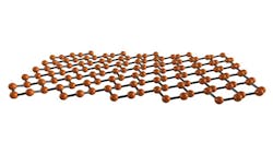
Researchers at the University of Texas (UT) at Austin’s Cockrell School of Engineering have created silicene (see the figure), a one-atom-thick layer of silicon. It has a hexagonal honeycomb structure. Silicene, like graphene, has been known but turning theory into actual material was a challenge that has now been overcome, at least on a small scale. Previously, very high temperatures were required to make small amounts of silicene.
UT’s Deji Akinwande teamed with Alessandro Molle at the Institute for Microelectronics and Microsystems in Agrate Brianza, Italy, and used a new method that initially limits the material’s exposure to air. The process starts with a block of crystalline silver in a vacuum chamber. Silicon is evaporated and condensed on the block. Next, a nanometer-thick layer of alumina is added. This allows a film of the layers of silver, silicone, and alumina to be removed by peeling them off the block. Silicene has also been grown on ZrB2 and iridium.
This film was transferred to an oxidized-silicon substrate for testing. Some of the silver was carefully removed so there were two silver electrodes on either side of the silicene sheet. This was done under vacuum conditions. The transistor was then tested. Subsequent tests in open-air conditions will follow.
The characteristics of silicene are still under investigation. Silicene can be used with different dopants to change the material and do things like tune the band gap of the material as is done with bulk silicon. In theory, it could be used to construct faster and more power-efficient transistors.
References:
One-Atom-Thin Silicon Transistors Hold Promise for Super-Fast Computing
About the Author
William G. Wong
Senior Content Director - Electronic Design and Microwaves & RF
I am Editor of Electronic Design focusing on embedded, software, and systems. As Senior Content Director, I also manage Microwaves & RF and I work with a great team of editors to provide engineers, programmers, developers and technical managers with interesting and useful articles and videos on a regular basis. Check out our free newsletters to see the latest content.
You can send press releases for new products for possible coverage on the website. I am also interested in receiving contributed articles for publishing on our website. Use our template and send to me along with a signed release form.
Check out my blog, AltEmbedded on Electronic Design, as well as his latest articles on this site that are listed below.
You can visit my social media via these links:
- AltEmbedded on Electronic Design
- Bill Wong on Facebook
- @AltEmbedded on Twitter
- Bill Wong on LinkedIn
I earned a Bachelor of Electrical Engineering at the Georgia Institute of Technology and a Masters in Computer Science from Rutgers University. I still do a bit of programming using everything from C and C++ to Rust and Ada/SPARK. I do a bit of PHP programming for Drupal websites. I have posted a few Drupal modules.
I still get a hand on software and electronic hardware. Some of this can be found on our Kit Close-Up video series. You can also see me on many of our TechXchange Talk videos. I am interested in a range of projects from robotics to artificial intelligence.

