Achieving reliable 3D ICs with die-level stress analysis
The rapid adoption of 3D integrated circuits (ICs) and heterogeneous packaging heralds a new era in semiconductor design. Benefits are clear: greater functional density, reduced footprint, and improved system performance. But these advances come with a cost—complex assembly structures introduce new forms of mechanical stress, threatening reliability at the die, package and device level.
The imperative for accurate 3D IC stress analysis
Vertical integration with multiple dies, interposers, varied materials and fine-pitch interconnects increases the potential for warpage, die cracking, solder fatigue and delamination. These failure modes can undermine both yield and long-term device performance. Compounding the challenge, many stress effects are subtle. Some only appear as degraded device mobility or latent circuit failures under temperature or mechanical cycling, rather than as overt physical defects.
Traditional 2D sign-off tools and even many package-level simulators fall short. They often oversimplify chip geometry, ignore localized effects inside advanced dies or disconnect package assembly conditions from downstream device behavior. In contrast, a multi-level stress analysis must encompass the full physical stack, capturing not only mechanical loads but also their electrical consequences.
Shift-left 3D IC stress analysis
Waiting until final assembly or sign-off to address stress risks can open the door to late-breaking issues—requiring costly layout changes, package redesign or even respins. Instead, shift-left verification strategies are becoming essential: by moving thorough reliability checks to earlier, more flexible stages in the design process, teams can spot and resolve critical vulnerabilities when the cost of change is lowest.
Designers of 3D ICs need early, automated analysis that supports rapid pathfinding and iterative package/device co-optimization.
Hierarchical, context-aware analysis for modern 3D assemblies
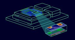
A chip-level 3D stress analysis software would model all elements of the packaged stack, from millimeter-scale substrates down to nanometer device regions. Automatically extracting die, layout and material information—including TSVs, bumps, interposers and underfills—the tool creates a detailed multi-scale physical representation for finite element analysis (FEA).
By simulating mechanical stress propagation throughout the assembly, engineers gain actionable insight into:
- Warpage and die deformation (figure 1)
- Stress concentration “hot spots” in critical die or package regions
- Mobility variations tied to piezoresistive effects
- Cumulative risks at chip-package and die-to-die interfaces
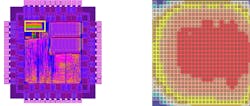
Figure 1. Example of die-level warpage in a 3D package, highlighting critical areas at risk for bump lifting, cracking or degraded device function.
Unlike legacy “black box” approaches that model the die as a simple silicon cuboid, designers of modern 3D ICs need granular, assembly-aware evaluation—ensuring no critical failure points go undetected.
Data-driven collaboration and iterative pathfinding
The early pathfinding stage of 3D IC design is often characterized by incomplete material data and evolving package specifications. These limitations can be addressed with modular input requirements. Teams can iteratively refine assumptions about technology layers, material stacks, and chiplet placement, using simulation results to drive collaborative tradeoffs between chip and package designers.
As the design matures, increasingly accurate definitions yield correspondingly precise stress profiles. Engineers can easily perform “what-if” analyses—repositioning key blocks or macro regions, or experimenting with alternative materials or process options to reduce warpage and improve reliability.
This approach brings the benefits of shift-left even closer: rather than fixing problems after fabrication, teams use up-to-date feedback to converge on optimal assembly choices before final package sign-off.
From simulation to sign-off: comprehensive stress visibility
As package components are finalized and die placements are locked, your 3D stress analysis software should scale to deliver full-stack, high-resolution stress analysis for sign-off verification. For example, the Calibre 3DStress software from Siemens EDA uses a trusted, thoroughly validated physical model that integrates stress impacts across every interface and material transition.
Visualization is key: the Calibre 3DStress tool generates detailed spatial maps of stress, warpage and marginalized regions, allowing targeted review by chip, packaging and reliability engineers alike (figure 2).
Figure 2. Stress distribution maps for a multi-die stack, with visual overlays of critical stress peaks and warpage zones relevant to device placement and circuit function.
Closing the reliability loop: electrical impacts and device-level modeling
A unique strength of Calibre 3DStress is its capacity to bridge mechanical analysis and electrical sign-off. By back-annotating physical stress data—including mobility shifts or piezoresistive perturbations—directly into netlists and device models, engineering teams ensure that both mechanical and circuit-level reliability are evaluated in tandem. This means “shift-left” not only for stress detection, but for comprehensive system verification.
Applications span a wide spectrum: automotive SoCs, data center processors, memory stacks, high-reliability products or any design where the interplay between packaging and circuitry determines success or failure over time.
Business and engineering impact
The demonstration of first-pass silicon success is a fundamental differentiator in today’s competitive semiconductor marketplace. By enabling design teams to resolve reliability risks upfront—rather than during late-stage debug or after manufacturing—Calibre 3DStress helps:
- Accelerate time-to-market by shortening debug and sign-off cycles
- Reduce risk of field failures, warranty claims, and costly respins
- Encourage more ambitious integration and feature partitioning without sacrificing reliability
- Optimize collaboration between chip and package, streamlining the full product lifecycle
Shift-left stress analysis and verification, empowered by detailed multi-physics modeling, is increasingly crucial for organizations that want a leadership position in 3D IC design and advanced packaging.
Conclusion
As heterogeneous 3D ICs become standard for system scalability and performance, comprehensive, early stress analysis moves from “nice to have” to mission critical. Calibre 3DStress brings together hierarchical physical modeling, automation, shift-left verification and electrical back-annotation to deliver robust, fast-turn insight from concept through sign-off. For engineering teams and business leaders alike, it’s a practical foundation for the next generation of reliable, manufacturable and innovative semiconductor products.
Sponsored By:

About the Author
Shetha Nolke, Principal Product Manager, Siemens EDA
Shetha Nolke is a Principal Product Manager at Siemens EDA, bringing 23 years of semiconductor innovation to her leadership in the Calibre 3D IC Physical Verification team, where she pioneers solutions for 3D IC Stress analysis. Drawing from her unique background as a former photomask fab line engineer at DuPont/Toppan Photomasks, she has spent the last ten years driving technical breakthroughs in the Calibre division. Known for her innovative problem-solving approach and talent for building collaborative teams, Shetha has become a driving force in advancing holistic solutions for the chip design community.
Comment About the Article
To join the conversation, and become an exclusive member of Electronic Design, create an account today!

Leaders relevant to this article: