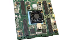
Virtex 7 FPGA-Based Prototyping System Brings Modular Advantage
Compactness, modularity, and cost optimization—key attributes in today’s IP verification and pre-silicon software development—are attainable with the proFPGA uno Virtex 7 FPGA-based prototyping system, according to developer PRO DESIGN. The IP development platform consists of the proFPGA uno motherboard and a variety of FPGA modules. Users can choose between proFPGA V7 FPGA modules, assembled with different Xilinx Virtex 7 FPGA devices (e.g., the XC7VX330T, XC7V585T, XC7VX690T, or XC7V2000T). Thanks to the system’s modularity, users can perform IP or design-parts development and then reuse the FPGA modules for SoC and ASIC prototyping by plugging the same modules and V7 FPGA modules on a proFPGA duo or quad motherboard. Maximum system speed is 400 MHz. Over standard I/Os, it’s possible to achieve single-ended point-to-point performance of up to 1.0 Gbit/s. When assembled with a proFPGA Xilinx Virtex 7 XC7V2000T module, the uno system has a capacity of up to 12M ASIC gates and eight extension sites. In addition, up to 1100 free FPGA I/Os are available to adapt standard proFPGA daughterboards or application-specific extension boards such as DDR3 memory, USB 3.0, Gigabit Ethernet, or PCIe Gen3.
