This file type includes high resolution graphics and schematics.
Firmware often is preprogrammed into flash memory devices prior to the printed-circuit board’s (PCB) manufacture to maintain high throughput and avoid slowing the manufacturing beat rate. Yet there are advantages to programming the flash memory after it has been soldered to the PCB. In-circuit test (ICT), the Joint Test Action Group (JTAG) interface, and external connectors all can be used to program flash devices without impacting manufacturing beat rates. Image size, existing manufacturing infrastructure, system capability, and required programming methods also should be considered in choosing an optimal preprogramming solution.
Table Of Contents
Onboard Programming Advantages
One of the most significant advantages of onboard programming is that it enables design and manufacturing engineers to combine IC testing and programming into a single manufacturing process, which eliminates the need to perform offboard programming of an IC prior to surface-mounting the device.
Related Articles
- Interview: Spansion’s CTO Talks About Embedded Charge Trap NOR Flash
- Design FAQ: Path To High-Performance NAND Flash
- Design FAQ: Reliability Challenges Emerge With NAND Flash Migration
Flash memory utilization typically depends on the development stage of a product. In many applications, designers use flash memory to develop, store, and eventually execute firmware and application code. Onboard programming is often used during the development of new application code or firmware. Code is written, compiled, and downloaded onto the flash device on the development board and then tested on the target PCB.
When the hardware and software nears production readiness, it is common practice to preprogram flash memory devices prior to starting high-volume PCB manufacturing flows for two principal reasons. First, firmware loaded onto the device can be used to perform basic booting and testing of the PCB during manufacturing to check system/module functionality. Second, loading the final firmware, operating system (OS), and application code on the flash device prior to manufacturing maintains a high-volume manufacturing beat rate. To support these usage models, multiple vendors provide systems for loading firmware and data into flash memory devices prior to the PCB solder flow process.
The ability to leverage existing manufacturing systems for testing, coupled with the fast program speeds of flash memory, make onboard programming a viable mainstream solution for programming flash memory. In addition to having no impact on the manufacturing line, other advantages of onboard programming include:
- Faster time-to-market: If a change is made to the flash memory image, the change can be sent directly to the manufacturing line, speeding the delivery time into production.
- Improved quality: Removing the preprogrammed inventory reduces the risk of sending out the wrong version of firmware, OS, or application code as well as the time and resources needed to track units that must be reworked.
- Supply chain simplification: Traditionally, manufacturing operations track both programmed and unprogrammed units, whereas with onboard programming, only unprogrammed flash units need to be monitored.
Onboard Programming Techniques
Several onboard programming (or in-system programming [ISP]) techniques are used to load firmware and data onto a flash device after solder reflow. These techniques include ICT, JTAG, and external connections (Table 1).
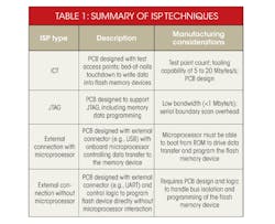
ICT is a test methodology that checks PCBs for assembly defects such as shorts, opens, resistance, and capacitance directly after devices are mounted in the solder reflow oven. After undergoing a successful test sequence, flash memory devices can be programmed directly by the ICT equipment. The program time must be very short (approximately 1 to 4 seconds) to avoid negatively impacting the manufacturing beat rate. In addition, programming a memory device with ICT typically requires a low-pin-count interface, which limits the number of nails/pins on the test fixture.
This file type includes high resolution graphics and schematics.
JTAG is an IEEE standard (IEEE 1149.1) that uses boundary scan architecture to test for structural integrity between devices on a PCB. The JTAG interface also can perform ISP of flash memory devices. During the boundary scan check, the interface enables direct control over the memory signals, enabling an image to be programmed into a flash device. JTAG programmers typically write software and data to the flash memory using data bus access similar to the access used to update CPU firmware.
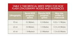
ICT and JTAG are typically used for programming small data images (less than 16 Mbytes) on flash memory devices like NOR due to the low bandwidth required by these processes (low-pin-count bus or slow clock frequencies). Table 2 compares the theoretical write performance of NOR flash lithography nodes and interfaces.
External connection and new ICT models are the best techniques for transferring larger data images that require a higher bandwidth. These two techniques provide an opportunity for manufacturing tool and support vendors to enable faster transfers of high-density firmware and data to flash memory devices. ICT testers have recently reached program speeds of 20 Mbytes/s.
External-edge connections accomplish onboard programming using two basic methods. With a microprocessor, data is transferred into the flash device with an existing connector (e.g., USB) using the main microprocessor on the PCB for control. Without a microprocessor, data is transferred into the flash device with an existing connector (e.g., UART) using specific control logic on the PCB dedicated to the manufacturing environment. In this case, the onboard microprocessor is not used.
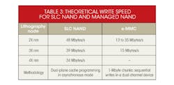
External connection techniques and new ICT models can transfer data at much higher rates. Table 3 shows the bandwidth that can be achieved using single-level cell (SLC) NAND and e∙MMC memory for a given lithography node. In each case, the device rather than the interface limits the programming bandwidth.
Critical Factors For Onboard Programming
When choosing an onboard programming method to program images on flash devices, memory type, image size, board design, and existing manufacturing capabilities are all critical factors to consider.
Firmware code, operating systems, and data files can range from tens of kilobytes to hundreds of megabytes. For a smaller image size (less than 8 Mbytes), ICT and JTAG are ideal because of their low bandwidth. Today, many manufacturing lines use JTAG and ICT to test board-level functionality, so additional tools are not needed. With existing hardware in place and NOR flash products that can program between 1 Mbyte/s and 2 Mbytes/s, onboard programming is an ideal solution when the program time does not exceed 4 seconds and does not impact the manufacturing beat rate.
The program performance of high-density (32 Mbytes to 1 Tbyte) NAND flash enables the use of optimized onboard programming techniques. SLC NAND is the fastest (5 to 60 Mbytes/s) programming flash memory on the market. However, the flash market is transitioning to managed NAND solutions such as e∙MMC embedded memory that have programming speeds ranging from 10 to 35 Mbytes/s.
Memory devices with high-bandwidth capabilities use two different techniques for transferring large data images: new ICT models and external connections. Recent ICT models can support fast program speeds for high-density memory devices. External-edge connectors can either use the onboard processor or skip the processor and program the flash memory directly. Both of these external connection techniques require either a PCB design to route the data through the processor or logic onboard to handle bus isolation to program the flash memory.
Conclusion
Integrating board-level testing and onboard programming into a single manufacturing process provides multiple advantages. The ability to send flash image updates directly to the manufacturing line accelerates time-to-market and reduces the risk of having outdated flash images in production, which helps to improve quality. In addition, reducing the number of preprogrammed and unprogrammed units that need to be tracked simplifies the supply chain.
The ICT, JTAG, and external connection techniques enable a processor to boot from the flash memory device and run PCB functionality tests immediately after solder flow. Given the benefits of onboard programming, it is worthwhile for system designers and manufacturing engineers to re-evaluate the flash programming process, especially considering that the future of image placement into flash memory is evolving from offboard to onboard programming, and future technologies, like phase change memory (PCM), will require onboard programming.
The optimal method for onboard programming depends on several factors, including existing manufacturing infrastructure, system capability, and the required programming type, such as small boot code and/or medium- to high-density code and data. It is important to consider all these factors and work closely with the product supplier, programming vendor, and OEM to choose the right solution.

This file type includes high resolution graphics and schematics.
About the Author
Brian Bradford1
Applications Engineer
Brian Bradford joined Micron in 2010 as an applications engineer with the Embedded Solution group. Prior to joining Micron, he started is professional career as a fab yield & integration engineer for Intel. He then stayed with Intel and moved to a technical marketing role for the Embedded Business Group, which was subsequently transferred to Micron Technology. He has a BS in chemical engineering and petroleum refinement from the Colorado School of Mines. He can be reached at [email protected].
Comment About the Article
To join the conversation, and become an exclusive member of Electronic Design, create an account today!

Leaders relevant to this article: