AMD Moves from HBM to LPDDR5X with New Memory-on-Package SoC
What you’ll learn:
- The differences between AMD’s new LPDDR5X memory-on-package (MoP) architecture and HBM.
- How hyperscalers are aggressively stockpiling AI chips, leading to HBM shortages and rising costs.
- How AMD’s MoP-based Versal increases memory capacity and bandwidth in a smaller form factor.
AMD introduced its first high-performance Versal SoC with a memory-on-package (MoP) architecture, integrating LPDDR5X to boost capacity and bandwidth without relying on increasingly scarce high bandwidth memory (HBM).
The MoP architecture integrates 32 GB of LPDDR5X, delivering up to 288 GB/s of bandwidth in up to 60% less space than a standard package with external DRAM. While it lacks the same flexibility as on-the-board LPDDR5X, AMD said the Versal Premium Gen 2 MoP improves performance while reducing the power and latency penalties that come with it. While it lacks the same level of bandwidth of in-package HBM, MoP balances things out by reducing the complexity, costs, and supply constraints that come with it (Fig. 1).
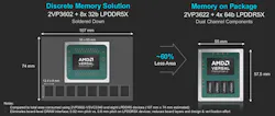
“We’re introducing memory-on-package as another step in the innovation stack,” said Mike Rather, senior product manager in AMD's Adaptive and Embedded Computing unit. The Versal MoP fits many of the same applications as its existing Versal Premium Gen 2. These include ultra-fast, terabit-per-second networking in data centers, high-bandwidth RF signal processing in wireless networks, and AI acceleration in aerospace and defense systems, all of which are pushing more data through tighter space and power budgets (Fig. 2).

The pivot also reflects the economic realities of HBM. The 3D-stacked memory is a core building block in AI accelerator chips and is broadly used in high-performance FPGAs. But rising demand for AI hardware is siphoning most of the HBM memory supply, leaving other markets — including embedded systems — to compete for what’s left. New generations of HBM are also largely being shaped by the needs and wants of hyperscalers such as Google, Microsoft, OpenAI, and Anthropic at the expense of embedded, said Rather.
By replacing HBM with LPDDR5X in the package, AMD aims to avoid the HBM shortages while still eliminating the board-level routing, power integrity, signal integrity, and other challenges that come with external memory.
Memory Dilemma: More Capacity, More Bandwidth, Less Space
According to AMD, its MoP technology is designed to address one of the core dilemmas facing embedded systems: delivering more memory capacity and bandwidth within strict size and power constraints.
“Memory is red hot,” said Rather. “Supply is constrained, which is being driven by the massive demand we're seeing from the giant wave of AI investments. Costs have been increasing, and there is a relatively small set of suppliers. This is impacting every part of our industry, because memory is one of the essential ingredients to embedded systems, and as those systems push to higher performance levels and infuse more AI, they tend to need more memory and more memory bandwidth.”
In many cases, embedded systems use FPGAs and other highly programmable SoCs such as AMD’s Versal because they bring both flexibility and deterministic, real-time performance to the table. But they also require larger memory capacities to store data close to the chip and more memory bandwidth to keep data movement from becoming a bottleneck on performance. On top of that, these systems are layering in a lot of AI workloads, which require more of both, said Rather.
One solution is to put HBM memory inside the processor's package, eliminating board-level memory interfaces and saving significant space on the PCB. AMD introduced its first Virtex UltraScale+ FPGA with HBM in 2018, integrating up to 16 GB of memory capacity and 460 GB/s of peak bandwidth. Then, in 2022, the company applied the same approach to its first HBM-equipped Versal SoC, increasing capacity to 32 GB and bandwidth to as much as 840 GB/s.
The HBM is connected to the main processor using 2.5D interposer technology. The silicon interposer serves as a sort of mini circuit board with high-density interconnects that link together programmable logic dies, also known as super logic regions (SLRs). Placing the HBM in close physical proximity to these SLRs reduces power consumption and latency during data movement, bypassing the "memory wall” that plagues traditional DRAM (Fig. 3).
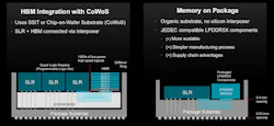
The advanced packaging technology, called chip-on-wafer-on-substrate (CoWoS) by TSMC, is the de facto standard for integrating HBM. However, it does add complexity and expense to the manufacturing process, said Rather.
The Restrictions on HBM in Embedded Systems
HBM offers many performance advantages between its high bandwidth, thanks to its wide parallel interface, and high density, thanks to its 3D stacked architecture. But, according to Rather, it also has a lot of disadvantages in embedded systems.
One of the more practical challenges is even procuring it. HBM surrounds some of the top AI accelerators, such as NVIDIA's Blackwell and AMD’s Instinct GPUs, and next-gen AI chips need exponentially more HBM per chip. Driven by hyperscalers aggressively stockpiling GPUs, memory-chip giants such as Micron, Samsung, and SK Hynix have sold out of HBM capacity for the foreseeable future. It’s triggered skyrocketing prices and spillover shortages in other areas that are severely restricting global hardware production.
HBM is also increasingly being designed to meet the demands of data centers over embedded systems, said Rather. These memory chips can typically tolerate continuous operating temperatures of up to 95°C and “excursion” temperatures of up to 105°C. Thus, they’re able to handle the heat typical in today’s AI server racks.
However, HBM chips can struggle to handle the harsh conditions outside of the data center. For instance, they're generally not qualified to operate at sub-0°C temperatures, according to AMD.
HBM is also evolving at a significantly faster pace than LPDDR5X to keep up with the bandwidth demands of AI. That rapid product cadence contrasts with the needs of embedded systems, many of which remain in service for more than a decade and depend on components remaining available for as long as 15 years.
MoP: Not-as-High-Bandwidth Memory Directly on the Package
AMD said the MoP-based Versal tackles a lot of these tradeoffs by placing LPDDR5X memory on the same organic substrate as the processor, rather than surrounding it with HBM mounted on a more advanced silicon interposer.
“It's a simpler approach where the connections are made in the organic substrate,” said Rather. “This is more scalable and provides manufacturing advantages as well as supply chain advantages. And these are JEDEC-compatible parts that we can qualify multiple vendors for.”
At the heart of the new Versal is a programmable logic die featuring up to 1.5 million look-up tables (LUTs) and all of the other building blocks of a processor in its class, including a dual-core Arm Cortex-A72 and dual-core Arm Cortex-R5. It also integrates a wide range of network interfaces including 600G Ethernet as well as on-chip accelerators such as the crypto engines, which are designed to run encryption in real-time on 400G networks (Fig. 4).
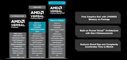
The integrated memory controllers connect to 32 GB of LPDDR5X on the organic substrate using short interconnects measuring 0.4 mm. In addition, the chip integrates CXL 3.1 and PCIe 6.0 with up to 2 Tb/s of total bandwidth across 16 lanes operating at 64 Gb/s per lane, enabling high-speed data movement. AMD said it also offers the flexibility to attach more memory with LPDDR5X support of up to 9,000 Mb/s and connectivity to CXL memory pooling and expansion modules.
Everything fits into a single 55- × 57.5-mm package, which saves 60% more space compared to off-package LPDDR5X. By eliminating board-level memory routing, AMD said the Versal MoP enables smaller form factors that are traditionally a tight fit for FPGAs, including 3U VPX for aerospace and defense applications, OCP for data centers, and PXI for test and measurement.
Rather noted that “the common thread is that all these implementations are packing an incredible amount of functionality into very small form factors.”
AMD said the MoP approach is also more secure since the memory interface is embedded in the package, eliminating board-level access to memory signals. The integrated memory controllers come with DDR memory encryption to protect data at rest without sacrificing programmable logic resources. It can also encrypt everything running through the PCIe 6.0 lanes, securing data in flight at the link layer to defend against physical attacks.
The Versal MoP also leverages JEDEC-standard LPDDR5X memory chips that are designed to handle harsh conditions, operating at industrial-grade temperatures ranging from −40 to 110°C. The LPDDR5X is also long-lasting, with 15 years of component availability, AMD said. Importantly, that helps decouple product availability from the short refresh cycles of HBM, reducing the risk of forced redesigns due to memory end of life or limited accessibility.
By bringing a pre-validated DRAM interface inside the package, AMD explained that the Versal MoP helps reduce board-level simulation and validation, shortening development cycles for engineers while reducing design risks and the chances for costly re-spins.
“It's one package, it's architected, it's designed, and it's validated,” said Rather. “You can short-circuit many of the steps you would need to implement a discrete memory interface.”
AMD will start sampling the new Versal SoCs at the end of 2026, with production shipments expected to begin in the second half of 2027.
About the Author
 James Morra
James Morra
Senior Editor
James Morra is the senior editor for Electronic Design, covering the semiconductor industry and new technology trends, with a focus on power electronics and power management. He also reports on the business behind electrical engineering, including the electronics supply chain. He joined Electronic Design in 2015 and is based in Chicago, Illinois.