Boosting Semiconductor Yield and ROI
IDMs and fabless semiconductor firms are working to get high-quality products to market fast, and they have a variety of software tools to assist them. They can choose design-for-manufacture (DFM), diagnostic, and yield-analysis tools that make use of scan-test and related data to identify faults and root causes to assist in physical failure analysis (PFA) and help optimize processes. In addition, they can employ tools that gather data from across the foundry and OSAT supply chain to maximize ROI.
DFM Tools
Cadence Design Systems offers DFM tools to aid with the development of manufacturing-friendly designs, according to Manoj Chacko, product marketing director for DFM products. The goal, he said, is to reduce the number of iterations at signoff prior to design tape-out. The rule-based and model-based DFM technologies have been integrated into Cadence’s implementation product solutions, forming what he called “in-design DFM,” which begins at standard-cell and IP design and extends through block-level and chip-level implementation for both custom and digital flows.
The DFM technologies, Chacko said, address the following areas: model-based random-defect analysis, model-based litho and chemical mechanical polishing (CMP) checks/analysis, turbo-litho and block-based CMP analysis, pattern search and matching, pattern search and classification, electrical variability for layout-dependent effect analysis on standard-cell libraries, layout-dependent effect analysis for custom implementation, and critical-path layout-dependent effect analysis and context-dependent placement for digital implementation.
Cadence, he said, can “demonstrate superior DFM convergence via in-design DFM built in the implementation tools and use the same technology as in the standalone DFM signoff products. In-design focuses on both electrical DFM and physical DFM.”
Yield-Learning Efforts
In addition, said Bassilios Petrakis, product marketing director for Cadence’s Encounter Test products, the company offers Encounter Test Volume and Precision Diagnostics to support yield-learning and time-to-market improvements. “These products,” he noted, “are key components of our Encounter Test offering, which also includes DFT Architect for scan logic and test IP insertion within the RTL Compiler synthesis cockpit and True Time ATPG for analysis and test-pattern generation.”
“Volume Diagnostics helps identify yield-limiting failures from logic diagnostics results,” he said, while “Precision Diagnostics allows concise diagnostics callouts for a particular failing die.” Together, these tools, he said, “help provide a means to monitor diagnostics results for design or library elements that appear to be causing yield excursions.” The tools also identify defect locations to assist in PFA.
Petrakis said the Encounter Test tools use the design database, failure data, and ATPG patterns together to create an accurate simulation environment to debug ATE failures. These tools, he added, can interface into physical layout tools like Cadence’s Virtuoso to help identify where the defects are located and the fault type.
According to Sagar A. Kekare, who handles product marketing in the Synopsys silicon engineering group, “We continue to observe that yield learning in nanometer nodes is gated largely by systematic failure mechanisms that stem from design or design-process interactions. This trend only keeps rising as we go to smaller geometries.” To address the challenges raised by this trend, Synopsys offers a design-centric yield-management approach.
Said Kekare, “We believe that yield-learning efforts are broadly divided into two categories: design-centric systematic yield limiter identification and fab-based inline defect reduction.” Synopsys’ solutions for these categories include, respectively, Yield Explorer and the Odyssey Defect Management System, both of which, Kekare said, have been adopted by top-tier and mainstream IDM, fabless, and foundry customers. With the two offerings working together, said Kekare, “We offer the full range of capabilities to use design information to rapidly isolate the most important systematic yield limiters, identify the specific design-process interactions responsible for the yield loss, and integrate these into the fab defect management so that customers may effectively target their inline defect-control efforts toward these yield limiters of high impact.”
Kekare explained that Yield Explorer automated volume diagnostics (AVD) reads in scan diagnostics data from Synopsys TetraMAX ATPG or other diagnostics tools, over multiple failing dies, and contrasts the data (the failing nets vs. passing nets) against all of the physical design. “This analysis methodology captures the true yield impact of any given design element (cell, instance, net, via, etc.) at 10x the speed of any other method, ensuring a focus on high yield impact locations in picking sites for PFA.”
At Semicon Europa, Synopsys and STMicroelectronics in a joint presentation1 concluded that systematic failure mechanisms in nanometer-node technologies dictate that test must feed yield-learning efforts and that volume diagnostics can provide the most rapid yield-learning solution. In addition, the presenters noted, “Different strategies must be considered for reducing the operational costs of volume diagnostics while sustaining a high yield-learning rate,” concluding that “sampling protocols for data collection and excursion capture provide a good path to cost reduction” and that early recognition of multivariate fault signatures also supplies a path to cost reduction.
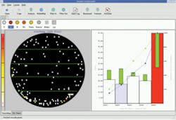
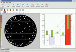
Courtesy of Mentor Graphics
Diagnostic-Driven Yield Analysis
Geir Eide, product marketing manager at Mentor Graphics, said Mentor offers what it calls “diagnosis-driven yield analysis,” which consists of two products: Tessent Diagnosis and Tessent YieldInsight (Figure 1). “Tessent Diagnosis,” he said, “identifies the location and type of defect for each digital semiconductor device that fails manufacturing test. Tessent YieldInsight analyzes the diagnosis results from a number of failing devices to separate random and systematic failures and identify the suspected root cause of yield loss.”
Eide said Mentor’s approach uses two forms of design data. Tessent Diagnosis uses a design description (logic and layout level) along with the production test patterns and ATE fail data to diagnose each failure. And in 2011, he said, “We expanded the concept of diagnosis-driven yield analysis through ‘DFM-aware yield analysis.’ This solution links the DFM analysis capabilities in Calibre YieldAnalyzer with the diagnosis analysis capabilities in the Tessent Diagnosis and Tessent YieldInsight products.”
Layout-aware diagnosis identifies defect location and classification for devices failing manufacturing test. “These diagnosis results are correlated with DFM analysis results and evaluated to identify and understand systematic yield loss and to determine if this yield loss is caused by DFM violations,” he added.
Eide said the Mentor approach leverages design information (both logical and physical) and production test results to identify the root cause of yield loss without relying on any fab data and before any PFA is performed. This is in contrast with other yield-analysis techniques that rely on expensive PFA techniques to correlate yield issues with the design features. The methodology, he said, reduces the cycle time to the identification of the root cause of yield loss by 75% to 90% and is compatible with any process technology or fab.
The approach, he said, also “gives fabless semiconductor companies, which typically have limited access to manufacturing process data, an opportunity to quickly separate design- and fab-centric yield limiters.” For IDMs and foundries, he said, the methodology complements traditional methods (such as yield management systems) and helps identify yield limiters (typically representing the last 1% to 2% in high-volume manufacturing) otherwise not found.
Limited access to relevant data in a multivendor supply chain is a major concern that vendors are trying to address. While Eide mentioned that fabless companies typically have limited access to manufacturing data, Kekare at Synopsys cited the alternative—lack of access to design data in the foundry: “Very early on we recognized that use of design data in a fabless-foundry environment is a topic of high sensitivity due to IP-protection concerns. We have developed a collaborative framework within Yield Explorer that fully addresses this sensitivity by not requiring transfer of any sensitive design data to the foundry while retaining all the benefits of using such design data in yield analysis.”
A related problem, of course, is who owns the problem that analysis of the data might reveal. “Historically, yield was always considered a manufacturing problem and the foundry’s problem,” said Eide at Mentor. “This is still often the case at mature feature sizes, although even at these nodes, fabless semiconductor companies in reliability-sensitive markets such as medical, MIL/aero, and automotive are eager to fully understand even minor yield issues.” In other markets, he said, as geometries move toward 40 nm and below, there is more variability between products, “which in turn makes it important for leading-edge fabless semiconductor companies to take ownership of yield analysis.”
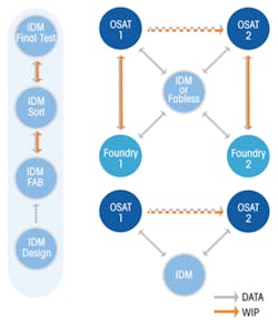
Courtesy of OptimalTest
Supply-Chain Visibility
OptimalTest’s approach, which complements the scan-based diagnosis and analysis approaches from the EDA companies, aims to break down barriers that hide useful data from the entities that can most effectively apply it to solve problems. Danny Glotter, founder and CEO of OptimalTest, said his goal is to pave the semiconductor information superhighway across the supply chain to support real-time data collection, secure data transfer, and data analysis. OptimalTest products serve fabless companies and IDMs operating in a fabless or fab-lite mode in which they outsource fabrication, assembly and test, or both (Figure 2).
Said Glotter, a fabless company designs and markets its products but does not engage in manufacturing, assembly, and test. That leads to the problem fabless companies have in trying to establish supply-chain visibility. To provide improved visibility, said Glotter, “OptimalTest works to interconnect a triangle of three parties—fabless companies like Qualcomm, foundries like TSMC and UMC, and OSATs like ASE and Amkor.”
The OptimalTest approach is gaining some traction, based on a presentation2 at last fall’s International Test Conference by Octavio Martinez, senior director of engineering at Qualcomm. Martinez placed the challenges in the context of Qualcomm’s requirements as the number 1 fabless company, number 1 wireless company, and number 1 RFIC company as well as one of the top 10 semiconductor suppliers.
Optimizing the test process—minimizing test time, optimizing NPI yield ramp, and maximizing coverage—requires visibility into actionable test data, Martinez said, likening that task to finding a needle in a haystack. Qualcomm accumulates 4 terabytes of data per quarter, he said, and the company looked to OptimalTest for assistance, launching a pilot program in 2008.
In addition to the huge volumes of data involved, challenges centered on multiple suppliers in different locations, inconsistent test environments, and inconsistent data formats. The challenges, Martinez said during his presentation, include providing connectivity to the manufacturing execution systems (MES) and other systems across the supply chain. In addition, a successful implementation would require management commitment, with management assured of a favorable ROI, and the project would need to be viewed as a “win-win” among Qualcomm and all participating companies in the supply chain. That requires buy-in from each organization’s IT department.
During his presentation, Martinez said that the engagement with OptimalTest as of last November has seen full deployment of the OptimalTest solution at final-test suppliers with extension to wafer-sort suppliers imminent. The deployment, he said, involves dozens of OSAT sites around the world on hundreds of testers. The result, he said, is a high level of data quality and consistency, with actionable data available in minutes to product and test engineers, yield engineers, operations personnel, and management.
Addressing 3-D ICs
OptimalTest and the EDA companies are all addressing yield issues that might arise with emerging 3-D chips.3 Said Eide at Mentor, “At smaller geometries, there is a dramatic increase in the number and complexity of design-sensitive defects. A picture of a defect (as a result of PFA) is no longer sufficient to understand the root cause.” Each new design, he said, brings additional variability and new defect types, and therefore, “One cannot rely on, for instance, test chips or other generic structures alone.”
PFA, Eide added, is still possible, but the cycle times and the costs increase. “From a yield and failure-analysis point of view, 3-D means even less visibility into the design with traditional methods,” he said. “Therefore, we expect that yield-analysis methods that are based on structural-test methods will be even more valuable for 3-D chips.”
Petrakis at Cadence takes a similar view. “As geometries shrink, PFA is having a harder time identifying the defects,” he said. “There are other more complex failure mechanisms that might not be easily seen in the physical design and only confirmed through simulation.”
He continued, “Regarding stacked dies, we believe that if the packaging yields are high for 3-D or 2.5-D chip modules, it becomes possible to produce a smaller die with higher yield and put multiples of them together to make the full product. Tossing bad die costs less when they are smaller and when their yields improve, so you don’t have to toss as many of them. Using three chips on a package instead of one or two large chips can greatly improve overall product yields as long as the packaging yields are high.”
Said Kakare at Synopsys, “From all the discussions we have had so far, the current test and diagnostics approach seems to be adequate to handle 3-D chips. Of additional interest is the idea of matching the component chips based on their individual sort test results;” that is, when combining a processor chip with a large memory chip, the speeds of the processor and memory chips should match.
This matching, he said, would seem like an easy thing to do with a small number of dies. However, in full production, it would require mapping speed bins and other parametric attributes from each chip and then adding SKU labels to each tested part to ensure that correct SKUs are brought together in the 3-D package. “Yield Explorer,” Kakare said, “has the capability to deal with very large amounts of data, label the SKUs based on multivariate clustering, and detect subtle shifts in production that are moving the SKU distributions one way or the other and possibly creating bottlenecks in final package volumes.”
Randy Hierbaum, vice president of sales at OptimalTest, said his company also can support 3-D devices and stacked die, and he concurred that matching chips appropriate to combine in a single package is important. “As we move forward,” he said, “we will use the data we collect to help cherry-pick quality grade and ensure our customers are putting only the highest quality parts into expensive 3-D and stacked packages.”
References
1. Tancorre, V., et al., “The Changing Role of Test in Accelerating Time-to-Yield,” Semicon Europa, Oct. 11-13, 2011.
2. Nelson, R., “Qualcomm Leverages OptimalTest Software for IC Test,” Rick’s Blog, EE-Evaluation Engineering, Oct. 24, 2011.
3. Nelson, R., “Addressing Interposer and TSV Quality Challenges,” EE-Evaluation Engineering, February 2012.
For More Information
About the Author
Comment About the Article
To join the conversation, and become an exclusive member of Electronic Design, create an account today!

Leaders relevant to this article: