Revolutionizing Micro- and Nano-LED Manufacturability
What you’ll learn
- How researchers are pursuing the manufacturability of arrays of micro-optical devices.
- How one team is roll-printing micro-LED arrays.
- How another team is growing nano-LEDs using perovskite materials.
The drive (or need) to make components, including optical devices, smaller and smaller quickly runs into a fabrication and production problem, as material and dimensional tolerances impede achieving high volume with acceptable yields. Researchers at two disparate institutions are addressing these issues with very different yet innovative approaches to LED manufacturing.
Roller Printing at University of Strathclyde
Micro-LED display technology is of great interest because it can produce highly accurate color rendering with high speed and resolution while using little power. For larger micro-LED displays, significant challenges exist in integrating millions of tiny LEDs—sometimes smaller than a grain of fine sand—onto an electronic control backplane.
Addressing this issue, researchers at the University of Strathclyde (Glasgow, Scotland) have demonstrated a continuous roller-printing process that can pick up and transfer over 75,000 micrometer-scale semiconductor devices in a single micro-LED array of 320 × 240 pixels and do so with very high accuracy. The new method enables creating large-scale arrays of optical components and could be used to rapidly manufacture micro-LED displays.
The researchers say that their technology can match the designed device layout with an accuracy better than one micron. The setup is also inexpensive and simple enough to be constructed in locations with limited resources. Because the printing process is continuous, it can be used to simultaneously print numerous devices, which makes it highly efficient for large-scale production.
LED Roller Printing Process
The approach starts with an array of tiny devices that are loosely attached to their growth substrate. The surface of a cylinder containing a slightly sticky silicone polymer film is then rolled over the suspended array of devices, allowing adhesive forces between the silicone and semiconductor to detach the devices from their growth substrate and array them on the cylinder drum.
The single-shot roller printing process sequence is straightforward (Fig. 1):
- The donor and receiver chips are placed on the translation stage with a separation equal to the circumference of the roller.
- The roller surface is brought into contact with the translation stage with enough vertical load to produce rotational motion of the roller induced by translation of the stage surface, without any mechanical slip.
- The translation stage moves with constant velocity so that first the donor chip passes under the roller and the devices are released from their suspended positions, ultimately adhering to the roller surface.
- The roller makes a complete rotation driven by the translation stage until it makes contact with the receiver.
- The devices on the roller surface make contact with the receiver chip and are transferred onto the surface from the roller.
The entire roller printing process takes 20 seconds, running with a translation stage velocity of 8 mm/s.
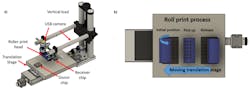
1. (a) Schematic representation of the roll printing setup. (b) Printing process (left to right), devices are released from a donor onto the roller print head and then released onto a receiver chip.
Test Results and Metrology System
The researchers tested the new approach with gallium-nitride-on-silicon (GaN/Si) semiconductor structures. They were able to transfer more than 99% of the devices in an array of over 76,000 individual elements with a spatial precision below a micron with no significant rotational errors.
An automated, submicron, precision metrology system was developed based on simple optical microscopy to assess such large device populations and allow for the assessment of yield. The automated system was designed to characterize the yield of the transfer process (assessment of missing membrane devices in a printed array) and the relative positional accuracy of the print (the device-to-device pitch as compared with the as-fabricated array) (Fig. 2). The image analysis was implemented in MATLAB and uses standard tools in the image-processing toolbox.
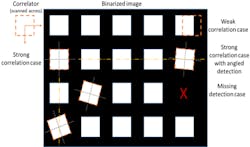
2. Schematic of the cross-correlation based metrology process: The image shows a binarized form of the optical microscope image, where the dotted square represents the ideal pixel form used to perform the cross-correlation assessment in x, y and θz dimensions. Examples of recognized device positions and missing device cases are shown.
"This printing process could also be used for other types of devices including silicon and printed electronics such as transistors, sensors, and antennas for flexible and wearable electronics, smart packaging, and radio-frequency identification tags," noted research team leader Eleni Margariti, who developed the new printing process. "It could also be useful for making photovoltaics and for biomedical applications such as drug delivery systems, biosensors, and tissue engineering."
The work is detailed in their lengthy (15 page) and well-written paper “Continuous roller transfer-printing and automated metrology of >75,000 micro-LED pixels in a single shot” published in Optical Materials Express from Optica (formerly Optical Society of America, or OSA). That page includes a link to an easier-to-read pdf version as well.
Halide Perovskites at MIT
Perovskites appear to be receiving major attention, somewhat similar to what’s happening with carbon nanotubes, as researchers deeply investigate their promise and potential, using them to solve ongoing challenges. Halide perovskites are a family of materials that have caught the eye of engineers for their superior optoelectronic properties and potential applications in devices such as high-performance solar cells, light-emitting diodes, and lasers.
These materials have generally been implemented into thin-film or micron-sized device applications. However, migrating them on-chip to function as light sources, photodetectors, and memristors is an ongoing challenge because they’re delicate and can easily be damaged by conventional fabrication and patterning techniques.
A team led by Farnaz Niroui, the EE Landsman Career Development Assistant Professor of Electrical Engineering and Computer Science (EECS) at MIT, devised an alternate approach to “grow” halide perovskite crystals in precise locations directly onto the desired surface where the nanodevice will then be fabricated.
Precision Well Placement for Nanocrystal Growth
Key to their process is that they localize the solution that’s used in the nanocrystal growth (Fig. 3). Using a lithographically patterned topographical template composed of wells with asymmetric surface wettability to confine the nanocrystal growth, they created a nanoscale template with small wells that contain the chemical process through which crystals grow. They modify the template surface and the inside of the wells, controlling wettability so that a solution containing perovskite material won’t pool on the template surface and will be confined inside the wells.
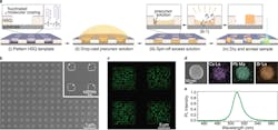
3. (a) Schematic illustration of the nanocrystal synthesis process: (i) Asymmetrically wetting template consisting of the non-wetting top surface and wetting well interior is fabricated using lithographic patterning of HSQ and selective surface treatment with fluorinated molecular assembly. (ii) CsPbBr3 precursor solution is drop-casted on the template. (iii) Excess solution is spun off of the template, leaving precursor solution localized in the wells. (iii-1) In each well, the solution forms a meniscus with a contact angle θ to the side walls. As the solvent evaporates, a nanocrystal nucleates in the well and continues to grow. The local variation in meniscus height δ results in a pressure gradient, leading to a force (F) directed from the highest (P0) to lowest (P1) pressure region, which helps guide nanocrystal positioning. (iv) Upon complete solvent removal through the evaporation process and an annealing step, the nanocrystal formation is complete. (b) SEM image of 1502 nm2 square wells containing CsPbBr3 nanocrystals patterned on Si substrate. Inset shows wells at higher magnification. (c) Fluorescent micrograph of four 12 × 12 arrays of 2502 nm2 wells patterned on SiO2/Si substrate. (d) SEM image and corresponding EDS maps of a single CsPbBr3 nanocrystal. (e) Photoluminescent (PL) spectrum of nanocrystals formed in a 2502 nm2 well.
Every detail is critical. For example, they found that the shape of the wells plays a critical role in controlling the nanocrystal positioning. If square wells are used, due to the influence of nanoscale forces, the crystals have an equal chance of being placed in each of the well’s four corners. For some applications, that might be good enough, but for others, it’s necessary to have a higher precision in the nanocrystal placement.
Instead, by changing the shape of the well, the researchers were able to engineer these nanoscale forces in such a way that a crystal is preferentially placed in the desired location. As the solvent evaporates inside the well, the nanocrystal experiences a pressure gradient that creates a directional force, with the exact direction being determined using the well’s asymmetric shape.
They also found they could control the size of the crystal that forms inside a well. Changing the size of the wells to allow for more or less growth solution inside generates larger or smaller crystals.
Nano-LED Array Fabrication
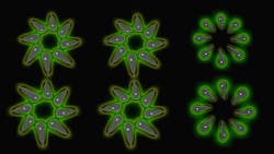
They demonstrated the effectiveness of their technique by fabricating precise arrays of nano-LEDs. In this approach, each nanocrystal is made into a nanopixel that emits light. These high-density nano-LED arrays could be used for on-chip optical communication and computing, quantum light sources, microscopy, and high-resolution displays for augmented- and virtual-reality applications.
They fabricated arrays of 600 to 2,400 nano-LEDs connected in parallel with an example array of 400 devices shown in the electroluminescence (EL) image (Fig. 4). In this example, a device was made using a teardrop-shaped well (specifically, a semicircle merged with a (20°, 80°, 80°) triangle of 1,000 nm2 area), which is formed within a 57-nm-thick SiO2 layer. The device design yielded perovskite nanocrystals of 214 ± 23 nm in the lateral dimensions.
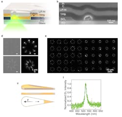
4. (a) Schematic illustration of the CsPbBr3 nano-LED formed using teardrop wells in a SiO2 topographical template. Note that the encapsulation isn’t visualized here. (b) Representative cross-sectional SEM image of a nano-LED. The C and Pt layers are deposited to protect the device during focused-ion-beam (FIB) cross-sectioning. (c) Meniscus profile in a teardrop well used as a nano-LED pixel. The meniscus results in an effective force for positioning the nanocrystal in the semicircular end. (d) Representative SEM images of nanocrystals formed in teardrop wells on a silicon substrate, where each teardrop well consists of a semicircle merged with a 10002 nm2 (20°, 80°, 80°) triangle (left). Electroluminescent (EL) images of nano-LEDs formed using the same design of wells taken under 10.5-V biasing voltage (right). (e) EL image of 400 nano-LEDs, arrayed in the two orientations shown in (d). (f) EL spectrum of the nano-LED array in (e).
The work is described in detail in their paper “On-site growth of perovskite nanocrystal arrays for integrated nanodevices” published in Nature Communications (it also has a link to a more-readable 9-page pdf). There’s also a 15-page Supplementary Information file.
About the Author

Bill Schweber
Contributing Editor
Bill Schweber is an electronics engineer who has written three textbooks on electronic communications systems, as well as hundreds of technical articles, opinion columns, and product features. In past roles, he worked as a technical website manager for multiple topic-specific sites for EE Times, as well as both the Executive Editor and Analog Editor at EDN.
At Analog Devices Inc., Bill was in marketing communications (public relations). As a result, he has been on both sides of the technical PR function, presenting company products, stories, and messages to the media and also as the recipient of these.
Prior to the MarCom role at Analog, Bill was associate editor of their respected technical journal and worked in their product marketing and applications engineering groups. Before those roles, he was at Instron Corp., doing hands-on analog- and power-circuit design and systems integration for materials-testing machine controls.
Bill has an MSEE (Univ. of Mass) and BSEE (Columbia Univ.), is a Registered Professional Engineer, and holds an Advanced Class amateur radio license. He has also planned, written, and presented online courses on a variety of engineering topics, including MOSFET basics, ADC selection, and driving LEDs.
Comment About the Article
To join the conversation, and become an exclusive member of Electronic Design, create an account today!

Leaders relevant to this article: