Advancing Memory: The Move to 3D NOR Flash

To truly appreciate the significance of this shift, one must first understand the differences between NOR and NAND memory. NOR flash is known for its fast random-access read speeds in demanding execute-in-place applications, high reliability, and functionality at extreme temperatures. It’s been a staple in applications where code storage is crucial, such as in automotive, cloud compute, and industrial systems, as well as in applications that might undergo multiple updates, e.g., over-the-air (OTA) transmission, due to its high write endurance.
Alternatively, NAND flash is preferred for data storage, offering higher densities at a lower cost per bit, but without the other NOR benefits. Thus, both devices solve unique challenges in their respective markets.
With the rise of artificial intelligence (AI), Internet of Things (IoT), and edge computing, the limitations of 2D NOR flash have become more apparent. These applications and their users require ever-higher densities while still depending on the benefits of NOR’s high reliability. The advantage of 3D NOR flash, therefore, comes into play—it addresses these challenges by delivering higher densities, greater scalability, and improved reliability.
Evolving Memory Needs: How 3D NOR Meets Market Demands
Today’s sophisticated applications, from AI-driven solutions to advanced driver-assistance systems (ADAS) in automobiles, require memory solutions that not only offer higher densities, but also deliver faster access times and greater reliability. Traditional 2D NOR flash, while effective in many applications, is reaching its physical and performance limitations. The planar architecture of 2D NOR flash constrains its scalability, making it challenging to meet the growing demands for higher-density and lower-latency memory.
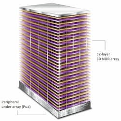
Conversely, by stacking memory cells vertically, 3D NOR flash overcomes the scalability issues inherent in the 2D NOR architecture. 2D NOR flash memory is able to achieve 512 Mb on a single die, so achieving higher densities would have to create a system-in-package (SIP) with multiple dies.
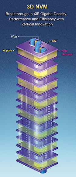
With 3D NOR, Macronix developed an architecture that can deliver 4 Gb on a single die. This vertical stacking enables significantly higher storage capacity within the same footprint, making 3D NOR an attractive solution for applications requiring large-scale nonvolatile memory (NVM) in space-constrained environments (Fig. 2).
By leveraging this architecture, end-system solution providers are able to reduce their need for multiple storage devices, such as eMMC and/or NAND. Moreover, 3D NOR flash offers shorter latency, thereby improving boot performance, which is an essential feature for applications that need near-instantaneous access to stored data.
Additional bonuses of this 3D NOR architecture are improvements to overall power consumption, since there’s less data transferring between separate memory devices, and improved security because fewer devices are susceptible to attacks. Furthermore, the improved reliability of 3D NOR flash, driven by its advanced architecture, suits it for industries where data integrity is paramount, such as in the automotive and industrial sectors.
3D NOR’s Technological Edge
3D NOR flash memory pushes the boundaries of what’s possible in nonvolatile memory. Its core technological advantages underscore how it could become a game-changer in the memory market:
8X density over 2D NOR
One of the most significant advantages of 3D NOR flash is its ability to achieve densities up to 8X greater than those of 2D NOR flash. As discussed earlier, the 3D architecture’s vertical stacking enables 4 Gb on a single die, whereas with 2D NOR, the maximum density capability is 512 Mb. The dramatic increase in density can store much larger datasets within the same physical footprint, addressing one of the most pressing challenges in today’s memory market (Fig. 3).
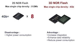
This 3D NOR architecture, therefore, will provide up to 8 Gb of storage, making it suitable for a wide range of memory-demanding applications from consumer electronics to high-end industrial systems.
QSPI and Octal Interface options
To ensure compatibility with existing systems and to maximize data-transfer rates, 3D NOR flash will need to support both Quad Serial Peripheral Interface (QSPI) and Octal Interface options per the JEDEC xSPI standard, which will be available with Macronix’s soon-to-be-introduced 3D NOR. These interfaces enable designers to easily integrate this new technology into their products without significant redesigns.
200-MHz double transfer rate
Speed is a critical factor in modern memory systems, especially for existing NOR customers requiring the additional density. 3D NOR flash addresses that by delivering a 200-MHz double transfer rate (DTR). This high-speed data transfer capability is essential for applications that require rapid access to large amounts of data, such as AI processing and real-time analytics.
Industrial and automotive temperature grades
Due to the diverse environments in which the memory products will be used, 3D NOR flash will operate across a wide range of temperatures. This aligns it for a broad array of markets and applications, including industrial and automotive, where extreme temperatures are a common challenge.
Bringing 3D NOR to Market: Timeline and Expectations
The introduction of 3D NOR flash marks a significant milestone for both the memory market and the global electronics industry. Companies such as Macronix expect to begin sampling 3D NOR flash chips in the second half of 2026, with full-scale production likely in 2027. By leveraging existing manufacturing facilities and processes used for developing 2D NOR, it will usher in the next generation of flash memory quickly and efficiently, while maintaining the quality and reliability standards.
Conclusion: 3D NOR is the Future
With the growing need for higher performance, increased storage capacity, and greater reliability, the constraints of traditional 2D NOR flash have become more apparent. The advent of 3D NOR flash presents a certain solution to these limitations, paving the way for the next generation of NVM.
At Macronix, we see 3D NOR flash as a key driver of the next wave of memory advances. We’re not only committed to ensuring a smooth transition to 3D NOR flash, but also setting the stage for the continued push of innovation in general NVM.
About the Author
Omar Mohammed
Technical Marketing Manager, Macronix America
Omar Mohammed is responsible for ecosystem, market, product, and business development at Macronix America. His previous roles include business management, project management, product development, and applications engineering. Omar holds a BS in Electrical Engineering, a BS in Computer Engineering, and a Minor in Technology Management from the University of California, Davis.
Comment About the Article
To join the conversation, and become an exclusive member of Electronic Design, create an account today!

Leaders relevant to this article: