Optimizing Reset Quiescent Current in Charge Sensitive Amplifiers

This article is in the TechXchange: Why Low Iq is the Smart Thing to Do.
Members can download this article in PDF format.
What you'll learn:
- What is a charge sensitive amplifier and what types exist?
- Use of a CSA ASIC in a Deep Underground Neutrino Experiment.
- Details regarding the Krummenacher feedback circuit for CSAs.
A charge sensitive amplifier (CSA) is a primary module of the front-end electronics of many types of silicon detectors, as well as most radiation detection systems. High gain, low input noise, and stability are the primary features of a typical CSA circuit to accomplish an amplified susceptible input charge (current) for added processing.
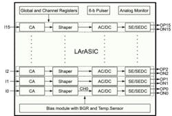
The CSA discussed in this article is a liquid argon ASIC (LArASIC) with a 16-channel front end, designed in a 180-nm CMOS process. This device was designed for full operation in a cryogenic temperature range spanning 77 to 89 Kelvin. This ASIC has 16 channels of charge amplifiers and shapers with a programmable gain and filter time constant that allows for measurement of weak charge signals from liquid argon Time Protection Chamber (LArTPC) sensing wires and PCB strips (Fig. 1).
This CSA ASIC will be used in a Deep Underground Neutrino Experiment (DUNE) (Fig 2).
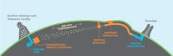
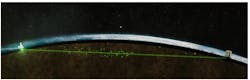
The primary science goals are (Fig. 3):
- Neutrino/antineutrino oscillations searching for the origin of matter.
- Supernova Neutrino bursts to learn about neutron stars and black holes.
- Proton decay to shed light on the unification of nature’s forces.
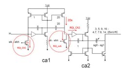
Because the detector sense wire’s leakage is negligible in the experiment, a tiny pre-bias current in the range of 100 pA to 5 nA, also known as reset quiescent current (RQI), is needed in each stage to set the dc quiescent point. RQI_CA1 (sinking) and RQI_CA2 (sourcing) are required at the inputs of the CA1 and CA2, respectively (Fig. 4).
The Krummenacher Feedback Circuit
The Krummenacher feedback circuit3 is quite well known and frequently employed in CSAs that are connected to dc-coupled semiconductor detectors. This unique circuitry provides a detector leakage current compensation along with a continuous reset in quite a simple structure dual functionality.
Another important issue that limits minimization of ASIC components is matching. In the smaller process feature size, the biggest impact will be on the close matching in the design of the circuitry.
The circuitry in Figure 5 shows the CSA with Krummenacher feedback. The Cd capacitance is critical for the stability of this circuit.
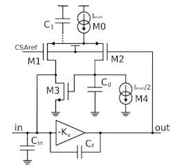
The circuit design demonstrated that a non-oscillating timing response was able to be achieved via the optimum selection of the CSA feedback capacitance as well as the total capacitance of the common source node in the Krummenacher feedback circuit. The crucial tradeoffs are noise and matching performance.
In applications where the detector leakage current is negligible, the Krummenacher network may not be the best choice. That’s because its current noise contribution (Sin) is proportional to the bias current, IKrum, while the shaping time is proportional to Qin /IKrum. Therefore, decreasing Sin will result in a shaping time increment. Any variation in input charge (Qin) will also directly change the shaping time.
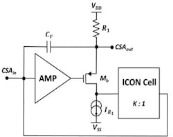
The drawbacks of the Krummenacher network can be overcome when the CSA is implemented with the use of a current conveyor (ICON cell) in the feedback network6 (Fig. 6).
Read more articles in the TechXchange: Why Low Iq is the Smart Thing to Do.
References
1. “Optimization of Charge Amplifier Reset Quiescent Current in LArASIC,” IEEE 2021.
2. “A 0.35µm Low-Noise Stable Charge Sensitive Amplifier for Silicon Detectors Applications,” Journal of Microelectronics, Electronic Components and Materials, Vol. 50, No. 1 (2020), pp. 3-13.
3 “Krummenacher Feedback Analysis for High-count-rate Semiconductor Pixel Detector Readout,” MIXDES 2010, 17th International Conference “Mixed Design of Integrated Circuits and Systems,” June 24-26, 2010, Wroclaw, Poland.
4. Update of TPC Electronics Development at BNL, 2020.
5. “High Time Resolution, Low-Noise, Power-Efficient, Charge-Sensitive Amplifier in 40 nm Technology,” Proc. XXXI International Scientific Conference Electronics - ET2022, September 13-15, 2022, Sozopol, Bulgaria.
6. C. Fiorini and M. Porro, “Integrated RC cell for time-invariant shaping amplifiers,” IEEE Transactions on Nuclear Science, Vol. 51, No. 5, pp. 1953-1960, 2004.
About the Author

Steve Taranovich
Freelance Technical Writer, Phoenix Information Communication LLC
Steve is a contributing editor to Electronic Design.
Author of the non-fiction “Guardians of the Right Stuff,” a true story of the Apollo program as told by NASA and Grumman Corp. engineers, an astronaut, and technicians.
Experienced Editor-In-Chief of EETimes/Planet Analog and Senior Technical Editor at EDN running the Analog and Power Management Design Centers from 2012 to 2019.
A demonstrated history in electronic circuit design and applications for 40 years, and nine years of technical writing and editing in industry. Skilled in Analog Electronics, Space-related Electronics, Audio, RF & Communications, Power Management, Electrical Engineering, and Integrated Circuits (IC).
1972 to 1988 worked as a circuit design engineer in audio (8 years) and microwave (8 years). Then was Corporate Account Manager/applications engineer for Burr-Brown from 1988 to 2000 when TI purchased Burr-Brown. Worked for TI from 2000 to 2011.
Strong media and communication professional with a BEEE from NYU Engineering in 1972 and an MSEE from Polytechnic University in 1989. Senior Lifetime member of IEEE. Former IEEE Long Island, NY Director of Educational Activities. Eta Kappa Nu EE honor society member since 1970.
Comment About the Article
To join the conversation, and become an exclusive member of Electronic Design, create an account today!

Leaders relevant to this article: