“Driving” GaN into High-Density Switching Power Supplies

This article is part of the TechXchange: Gallium Nitride (GaN).
Gallium nitride (GaN) continues to gain ground in power electronics. Not only does the technology eliminate reverse recovery, but it reduces losses at the high switching frequencies that matter to industrial- and automotive-grade power supplies.
However, it can be a challenge to take full advantage of the fast switching and other unique properties of GaN without more careful control and driving of the power FET. As a result, power semiconductor vendors look to upgrade their gate drivers to deliver more accurate, efficient power conversion.
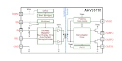
The AHV85110 is the latest isolated gate driver from Allegro MicroSystems purpose-built for GaN FETs. It’s not unlike other gate drivers for GaN: It delivers high sink and source currents with fast propagation delay and without being impaired by high-voltage transients. But its most distinctive feature is that it integrates an isolated dc-dc power supply directly, driving GaN FETs in footprints up to 40% smaller.
The unique architecture of the gate driver—the first product in Allegro’s Power-Thru family—helps reduce electromagnetic interference (EMI), which contributes to claims of up to 40% higher efficiency (Fig. 1).
By relocating the power supply from the printed circuit board (PCB) to inside a system-in-package (SiP), Allegro said the AHV85110 is relatively easy to integrate in high-voltage systems. The company cited everything from on-board chargers (OBCs) in EVs, uninterruptible power supplies (UPS) in data centers, and micro-inverters for converting solar, wind, and other types of renewable energy and exchanging it with the grid.
It’s critical to choose the right gate driver because of the role it plays in power electronics. The driver serves as the interface between the microcontroller (MCU)—that pumps out pulse-width-modulation (PWM) signals to control a power supply’s duty cycle, frequency, dead time, and phase-shift—and the power FET. Isolation is important for gate drivers to protect the system, and anyone close to it, against hazardous high voltages.
“We see SiC and GaN becoming the standard in power switches, and so we need to make sure we can support them with gate drivers,” said Ram Sathappan, Allegro senior director of applications marketing.
Breaking with Tradition
Traditionally, the gate driver is paired with a separate dc-dc bias supply or bootstrap diode to deliver the voltage that controls and drives the gate of the GaN or other FET on the high side of the power stage. Since the switching speed and quality of output power can affect performance, care must be taken when choosing power FETs, matching them to gate drivers and bias supplies, and then linking everything up.
High-density power supplies tend to be equipped with several gate drivers, each delivering a different voltage for each of the power FETs in the design. Every external bias supply paired to a gate driver adds transformers, filters, and other bulky components that then become potential points of failure. Choosing the best combination and routing them all together inside a DC-DC or AC-DC converter is no easy feat.
What’s more, GaN is opening the door to a wide range of new power-supply topologies—those that can harness the better switching capacitance and reverse-recovery losses of GaN but that are impractical with silicon MOSFETs and IGBTs. These topologies inevitably require a more complex interplay of analog, power, and passive components to function and, thus, more power rails to move voltage and current around it.
“The problem we’re addressing is in the power-supply design,” said Sathappan. “The power rails and the bias supply is where most of the complexity is and where you spend most of your time on a new design.”
When assembled, the connections between the gate driver, bias supply, and FET can induce common-mode capacitance between the control ground and the source terminal of the gate-driver controls, leading to high switching losses. Stray capacitance can also result in unwanted noise and electromagnetic interference (EMI) that can take a toll on a system and impede its electromagnetic compatibility (EMC).
Powering “Thru” Problems
Allegro is trying to cut through the complexity with its new Power-Thru isolated gate-driver technology.
The Power-Thru gate driver at the heart of the AHV85110 is unique in that it enables the transfer of the signal used to control the turn-on and turn-off cycle of the power FET and the power required to drive the FET’s gate. A tiny transformer in the package serves as the isolation barrier, making it possible to safely and efficiently transfer power and signals between the low- and high-voltage domains of a design.
Allegro said that Power-Thru eliminates the need for an external power supply and digital isolator for PWM signal isolation, both of which typically add extra cost, volume, and weight to the system.
Integrating signal isolation and bias power supply with the gate driver reduces the number of parts in a design—more than half the components in a typical implementation can be removed with the AHV85110, said Allegro—as well as the number of power rails linking them. The claim? Space savings of up to 40% on the PCB (Fig. 2). The gate driver itself is housed in a compact 12-pin, 10- × 7.6- × 2.4-mm package.

Packing everything in closer proximity reduces the distance that power and signals travel between the gate driver, bias supply, and power switch. The shorter connections limit the parasitic capacitance and inductance that can occur between the primary and secondary sides of a system due to the high dv/dt switching nodes. As a result, it’s unnecessary to use large and relatively heavy EMI filters.
Power-Thru also curtails excess power losses that occur through repetitive charging and discharging of the capacitance between the high-voltage bus and ground, according to the company. These parasitics can inadvertently cause high-voltage spikes that could lead to destructive events or create various other difficulties.
The AHV85110 integrates several protection features, including undervoltage lockout on the primary and secondary bias (VDRV) rails, internal pull-down on the input and output-drive pins, and fast response on the “enable” pin.
Inside the Package
With switching frequencies of more than 100 kHz, GaN FETs can run significantly faster than MOSFETs and IGBTs, opening the door for designers to use smaller, lighter passive components and magnetics.
To make sure power efficiency isn’t sacrificed at fast switching speeds, Allegro said the AHV85110 pumps out a peak source current of 2 A and a sink current of 4 A to enable rapid turn-on and turn-off of the FET. The result is a steep reduction in switching losses. The gate driver contains separate pins to set independent “on” and “off” resistors to adapt it to the switching characteristics of the specific GaN FET.
With a supply voltage of 10.5 to 13.2 V, the gate driver also features a fast propagation delay. This makes for a more accurate reproduction of the desired power switching waveform with higher fidelity in response to the PWM signal from the MCU. The company said a short propagation delay is preferable because it enables tighter and easier dead-time management between the on and off cycles of the FET.
The AHV85110 can also drive a floating switch in any location in a switching power topology, including totem-pole PFC, half-bridge, full-bridge, LLC, and various other DC-DC and AC-DC converter designs.
GaN power FETs run at higher frequencies than MOSFETs and IGBTs without losing inordinate amounts of power during the transition. But failure to protect against high-voltage transients that can happen at these high speeds may cause false turn-ons or damage to the system. Featuring isolated output pins for both bias power and drive current, the automotive-grade gate driver can also tolerate transients (CMTI) of up to 100 kV/µs, which is valuable in systems that require robust isolation, level shifting, or ground separation.
The other target for the AHV85110 is multi-level power converter topologies that string together several GaN FETs to handle higher bus voltages, while limiting the rated operating voltage of each FET. In general, GaN is unable to stand the stress when subjected to voltages of more than 650 V, potentially leading to failures. But the stress can be significantly reduced by spreading it out over more GaN FETs.
Allegro said Power-Thru is a fit for these advanced power-supply topologies because it prevents power rails from multiplying to manage the additional FETs, which are stacked for higher efficiency.
And, as Sathappan pointed out, “as you climb to higher voltages, these designs are only going to get more complex.”
Read more articles in the TechXchange: Gallium Nitride (GaN).
About the Author

James Morra
Senior Editor
James Morra is the senior editor for Electronic Design, covering the semiconductor industry and new technology trends, with a focus on power electronics and power management. He also reports on the business behind electrical engineering, including the electronics supply chain. He joined Electronic Design in 2015 and is based in Chicago, Illinois.
Comment About the Article
To join the conversation, and become an exclusive member of Electronic Design, create an account today!

Leaders relevant to this article: