DC-DC Converter Design Basics (Part 1): Buck Converters
This article is part of the Power Management series: DC-DC Converter Design Basics.
Members can download this article in PDF format.
What you’ll learn:
- The theory of buck converter operation.
- How to build buck converters using the SLG47105.
- Discover real-life examples where these devices can be used.
DC-DC converters are widely used to efficiently produce a regulated voltage from a source that may or may not be well-controlled to a load that may or may not be constant. This article shows how DC-DC converters can be built using the Renesas SLG47105 GreenPAK programmable mixed-signal matrix.
DC-DC converters are high-frequency power-conversion circuits that use high-frequency switching and inductors, transformers, and capacitors to smooth out switching noise into regulated DC voltages. Closed feedback loops maintain constant voltage output even when changing input voltages and output currents. At 90% efficiency, they’re generally much more efficient and smaller than linear regulators. Their disadvantages are noise and complexity.
DC-DC converters come in non-isolated and isolated varieties. Isolation is determined by whether or not the input ground is connected to the output ground. This three-part series will only describe the non-isolated converters (buck, boost, and buck-boost), but the IC capabilities allow for designing the isolated ones as well.
A buck converter steps voltage down, producing voltage lower than the input voltage. For example, a buck converter could be used to charge a lithium-ion battery to 4.2 V from a 5-V USB source.
A boost converter steps voltage up, producing voltage higher than the input voltage. A boost converter could be used to drive a string of LEDs from a lithium cell or provide a 5-V USB output from a lithium cell.
A buck-boost converter steps a voltage up or down, producing a voltage equal to, or higher or lower than, the input voltage. A buck-boost could be used to provide a 12-V output from a 12-V battery. A 12-V battery’s voltage can vary between 10 and 14.7 V. A buck-boost could also power an LED from a single cell. An LED forward drop is about 3.2 V. A lithium battery cell can vary between 2.5 and 4.2 V.
Buck Converter
A buck DC-DC converter, also called a step-down DC-DC converter, is a DC-DC power converter that lowers the output voltage while increasing the output current (Fig. 1).
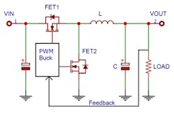
It consists of at least four components:
- Power transistor used as a switching element (FET1)
- Synchronous rectifier (FET2)
- Inductor (L) as an energy-storage element
- Filter capacitor (C)
The relationships between input and output voltage, current, and power are as follows:
- VOUT < VIN
- IOUT > IIN
- POUT = PIN – PLOSS
Theory of Buck-Converter Operation
When each cycle begins, FET 1 turns on first and the inductor current is determined by comparing the feedback loop voltage to an internal reference. When the sense voltage drops below the reference, FET 1 turns off and FET 2 turns on for the remainder of the cycle. FETs 1 and 2 turn on and off alternately, behaving like a typical synchronous buck regulator. The duty cycle of FET 1 increases until the maximum duty cycle of the converter reaches 94% to 98%.
As an example, a simple buck converter was designed using the SLG47105 IC and Go Configure software (Fig. 2). It has the following parameters:
- Input voltage range (VIN): 3.6 to 5.5 V
- Output voltage: 3.3 V
- Output current range: 0.5 to 1 A
- PWM frequency: 200 kHz
- Overcurrent/short-circuit protection: Internal OCP
Calculated values:
- Rated peak withstand current (IPK) : 2 A
- Inductance (LMIN) : 2 µH (2.2 µH, 2.5 A rated)
- Filter capacitor (C) : 25 µF (47- to 100-µF low ESR capacitor is recommended)
Go Configure Project
The regulator uses a 200-kHz clock, which is OSC1 25 MHz divided by 125 using the flexible divider (Fig. 2, again). This frequency was chosen as a compromise between two requirements:
- The highest possible frequency so that the smallest inductance coil and filter capacitor could be used.
- Low-enough frequency to ensure the highest efficiency of the HV outputs.
The buck pulse-width-modulation (PWM) logic is built on MF4 (CNT4/DLY4 and DFF 13) and 2-bit LUT2. The CNT4/DLY4 sets the maximum duty cycle of 96.6%. It remains at maximum until the feedback signal from the ACMP0H through 2-bit LUT2 cuts it. This regulates the output voltage.
It’s also possible to use one of two digital PWM microcells within the IC. However, since they're only 8-bit macrocells, the output voltage stability will be limited to PWM steps plus ACMP input offset voltage:

where:
- Δvout = output voltage drift
- Vref = internal voltage reference
- G = ACMP IN+ gain
- Voffset = ACMP input offset voltage
On the contrary, if using an analog PWM built on MF4 (CNT4/DLY4 and DFF 13) and 2-bit LUT2, the output-voltage stability will be limited to ACMP input offset voltage only. It should be mentioned that several factors increase the output voltage instability, such as macrocell propagation delay and other parasitic parameters. The final result will be a bit worse.
The HV OUT CTRL0 macrocell is configured as a fast-slew-rate half-bridge output. It has two half-bridge outputs which are connected in parallel to handle higher output current. Output pins (pins 7 and 8) are configured to «High and Low side on».
The ACMP0H in this design is used in a voltage feedback loop so that the PWM could stabilize the output voltage. The output voltage is determined by the ACMP’s Vref and the IN+ internal voltage divider. In this case:

where:
- Vref = internal voltage reference
- G = ACMP IN+ gain
The flexibility of the SLG47105 allows for the building of either two converters, using the HV OUT CTRL1 and ACMP1H as well, or connecting all HV outputs together for even higher output currents.
Conclusions
As can be seen, designing and building buck converters using the HVPAK SLG47105 chip is quite easy. The amount of unused macrocells leaves plenty of room for modifications and adding new features for proposed designs.
For example, a soft-start where a PWM period slowly increases from 0 to the required value reduces a peak startup current, programmable overcurrent protection, multiple output voltages, etc. Also, the HV OUT pins are suitable for driving external MOSFETs, which allows for building a very high-power DC-DC converter.
References
Circuit Design Software: Go Configure Software
Design Files: https://www.renesas.com/document/scd/cm-358-gp-file
About the Author
Nazar Sliunchenko
Technical Documentation Manager, Renesas Electronics
Nazar Sliunchenko graduated from National University "Lviv Polytechnic" in 2008, studying at the Department of Telecommunications, Radioelectronics & Electronic Engineering. He has more than 15 years of experience in hardware design, including analog and digital devices. Currently, Nazar is managing one of the Technical Documentation departments at Renesas Electronics Corp.
Comment About the Article
To join the conversation, and become an exclusive member of Electronic Design, create an account today!

Leaders relevant to this article: