The Journey to Low Iq in Bandgap References

This article is in the TechXchange: Why Low Iq is the Smart Thing to Do.
Members can download this article in PDF format.
What you'll learn:
- What are the key specs for a bandgap reference?
- Details regarding the error amplifier.
- The architecture of a conventional bandgap reference.
- The ingredients for a successful bandgap-reference solution.
Modern-day CMOS converters typically operate from 3.3- or 5-V power supplies. This will limit the on-chip voltage reference to a bandgap reference.
Reference technology in integrated circuits (ICs) is typically divided among three key product solutions: bandgap, buried Zener, and XFET references. This article will focus on the bandgap reference (BGR).
Bandgap Reference
Bandgap references need a high power-supply rejection ratio (PSRR), low quiescent current (Iq), low temperature coefficient (TC), and high accuracy. These references are composed of two transistors, each with different emitter areas that are used to generate a voltage proportional to absolute temperature (Fig. 1).1
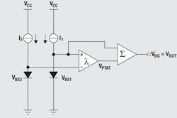
VBE1 and VBE2 will have opposite temperature coefficients. The VCC is converted to currents I1 and I2, which are mirrored to the output branch. The output Equation 1 is:
VO = VBE1 + ʎ(VBE1 - VBE2) (1)
where λ is the scale factor, VBE1 is the base-emitter voltage that’s the larger of the two transistors, and VBE2 is the base-emitter voltage of the second transistor.
Bandgap references, usually employed in systems up to 12 bits, produce a fixed (constant) voltage even in the presence of power-supply variations, noise sources, temperature changes, or circuit loading from other devices in a system. They rely on a ∆VBE in series with the temperature coefficient of a forward-biased diode junction.
Buried Zener-diode-based references employ a Zener diode and a forward-biased diode that’s connected in series. This combination leads to a near-zero temperature coefficient, long-term stability, and low-noise performance.
Let’s take a look at the error amplifier in a low-dropout (LDO) regulator, which needs a very stable reference voltage for equivalent measurements.
Error Amplifier
An error amplifier for frequency compensation may be just a simple voltage-to-voltage amplification device, such as a traditional op amp. The op amp will require local feedback between its output and inputs to ensure stability.
Error amplifiers can also be voltage-to-current amplification devices, i.e., the gm op-amp (operational transconductance amplifier, OTA). This is an open-loop amplifier stage that has no local feedback.
Researchers have offered some strategies that would improve the power efficiency and transient response performance of output capacitorless LDO regulators. Two main approaches were proposed:
- Modifying the error amplifier to improve the slew rate (SR).
- Using a capacitor coupling effect for fast transient response performance.
Unfortunately, these methods will necessitate additional circuitry and higher current, leading to a serious degradation in power efficiency. Let’s see how we can further modify and improve the error amplifier.
A high-performance OTA can function as an error amplifier with single-pole characteristics. An OTA has a differential input voltage that will lead to the production of an output current. It’s primarily used as a controlled-gain block. To bring stability to such an op amp, designers need to provide local feedback that’s between the input and the output of the device.
An Ultra-Low-Iq BGR
Extending battery life in handheld devices, implantables, and handheld devices is especially crucial in devices where charging or replacing is quite difficult and in many cases not possible. The silicon area must also be reduced.
On this front, a BGR architecture using a 130-nm TSMC CMOS technology offers a resistor-less topology. Powered via a 1.8-V power supply, it reduces circuit board area and consumes a minimal current consumption of 1.6 nA.
This switched resistor-less bandgap reference uses a single bipolar junction transistor (BJT) with cascaded stages of NMOS cascodes that will generate the necessary reference voltage. Ultra-low-Iq design techniques have been used in this design without sacrificing the TC and PSRR.
A Conventional BGR
The design architecture in a conventional BGR requires a proportional-to-absolute temperature (PTAT) voltage added to a complementary-to-absolute-temperature (CTAT) voltage. The PTAT voltage is generated from the difference between the base-emitter voltages of two BJTs having different emitter areas, making the reference voltage temperature-independent. The CTAT voltage is generated by a BJT base-emitter voltage. The reference voltage is now made independent of temperature:
VREF = Vbe1 + (R3/R2)VT ln(n) (2)
where n is the ratio of the emitter areas of transistors Q1 and Q2. The correct values of n, along with the ratio between resistor values, will give a zero TC at room temperature. (Caveat: matching constraints and area will deem it difficult to reduce Iq simultaneously with the low TC.)
The design will avoid using BJTs; instead, all-MOSFET BGRs will be utilized. That’s because while the BJTs have a low Iq and small area, they actually generate CTAT voltages using MOSFETs in the sub-threshold region, making them quite susceptible to variations in process.
Ultimately, other variations of bandgap-reference designs were pursued. However, all efforts proved to be lacking the goal for ultra-low Iq with low TC without sacrificing the area, PSRR, and other variations.
Proposed Successful BGR Solution
This solution targeted an ultra-low Iq with a low TC while not sacrificing board area or PSRR (Fig. 2).
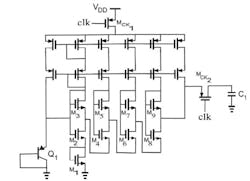
The design has a PTAT voltage that’s generated via cascading self-cascode NMOS cells. The CTAT voltage is generated from the bipolar transistor Q1. And the MCK1 drives the circuit ON and OFF from a low-frequency clock (clk).
CTAT Voltage Generation
In Figure 2, M1 and M2 have different lengths and widths, but they don’t have different threshold voltages when the source and bulk are connected to each other. This results in the Q1 VBE not equally divided between them, depending on the factor R. The gate-source voltage of M1 is given by:
VGS,M1 = RVBE, Q1/2 (3)
PTAT Voltage Generation
In a self-cascode NMOS cell that has transistors operating in the sub-threshold region, the drain-source voltage of the lower transistor in Figure 2 is:
VDS,bottom = nVTln(IbottomStop/ItopSbottom) (4)
where n as the MOSFET sub-threshold slope; VT is the PTAT thermal voltage; Itop is the drain current of the top transistor (M3, M5, M7, or M9 shown in Fig. 2); Ibottom is the drain current of the bottom transistor (M2, M4, M6, or M8 shown in Fig. 2); and Stop and Sbottom are the sixing factors of the top and bottom transistors, respectively.
The Voltage Reference
We generate the voltage reference by adding VGS,M1 to the drain-source voltage of the four bottom transistors in the self-cascode cells (PTAT). The voltage reference equation is:
VREF = VBE, Q1/2 + nVTln(S3S5S7S9/ S2S4S6S8) (5)
The TC gets set to zero at room temperature via the proper sizing of the transistors.
Switching
By adding transistors MCK1 and MCK2, the system will periodically turn the BGR ON and OFF. The BGR is able to use a low-frequency clock, which will typically be available in the system. When the clock is high, the BGR turns OFF and no current will be drawn from the power supply; when the clock is low, the reference voltage is generated and stored on the C1 capacitor.
The reference voltage will still be stored on C1, which is separate from the BGR to ensure correct operation. If the clock duty cycle is reduced, the quiescent current will be further reduced as well. However, the output ripple must be tolerable and the BGR must have enough time for startup.
Summary
Bandgap references are temperature-independent voltage reference circuits that are widely used in integrated circuits. The BGR will produce a fixed voltage even in the presence of power-supply variations, circuit loading from devices, as well as during temperature changes.
This BGR circuit concept was initially published by David Hilbiber in 1964: “A new semiconductor voltage standard,” IEEE Conference Publication. Hilbiber found that using the avalanche diode as a reference voltage source, was well known in the art. Hilbiber said, “If suitable precautions are taken, it has been found possible to obtain short-term stabilities of 10-50 ppm over moderate ranges of temperature.”
Choosing devices that are able to provide as much as 1,000+ hours of long-term operation can be quite challenging, especially when system functionality needs are complex. Today’s BGRs offer a quantum leap in performance.
Read more articles in the TechXchange: Why Low Iq is the Smart Thing to Do.
References
1. “Precision voltage references,” Texas Instruments.
2. “Tips and Tricks for Designing with Voltage References,” Texas Instruments, 2021.
3. “An 18-nA Ultra-Low-Current Resistor-Less Bandgap Reference for 2.8 V–4.5 V High Voltage Supply Li-Ion-Battery-Based LSIs,” IEEE Transactions on Circuits and Systems—II: Express Briefs, Vol. 67, No. 11, November 2020.
4. “Demystifying Type II and Type III Compensators Using Op Amp and OTA for DC/DC Converters,” Application Report SLVA662, Texas Instruments, July 2014.
5. “Substrate leakage current influence on bandgap voltage references in automotive applications.”
6. “Substrate leakage compensation technique for low quiescent current bandgap voltage references.”
7. “Understanding and Applying Voltage References,” Linear Technology, November 1999.
8. “A 1.6 nA Quiescent current Bandgap Reference in 130 nm CMOS Technology,” IEEE 2015.
About the Author

Steve Taranovich
Freelance Technical Writer, Phoenix Information Communication LLC
Steve is a contributing editor to Electronic Design.
Author of the non-fiction “Guardians of the Right Stuff,” a true story of the Apollo program as told by NASA and Grumman Corp. engineers, an astronaut, and technicians.
Experienced Editor-In-Chief of EETimes/Planet Analog and Senior Technical Editor at EDN running the Analog and Power Management Design Centers from 2012 to 2019.
A demonstrated history in electronic circuit design and applications for 40 years, and nine years of technical writing and editing in industry. Skilled in Analog Electronics, Space-related Electronics, Audio, RF & Communications, Power Management, Electrical Engineering, and Integrated Circuits (IC).
1972 to 1988 worked as a circuit design engineer in audio (8 years) and microwave (8 years). Then was Corporate Account Manager/applications engineer for Burr-Brown from 1988 to 2000 when TI purchased Burr-Brown. Worked for TI from 2000 to 2011.
Strong media and communication professional with a BEEE from NYU Engineering in 1972 and an MSEE from Polytechnic University in 1989. Senior Lifetime member of IEEE. Former IEEE Long Island, NY Director of Educational Activities. Eta Kappa Nu EE honor society member since 1970.
Comment About the Article
To join the conversation, and become an exclusive member of Electronic Design, create an account today!

Leaders relevant to this article: