DC-DC Converter Design Basics (Part 3): Buck-Boost Converters

This article is part of the Power Management series: DC-DC Converter Design Basics.
Members can download this article in PDF format.
What you’ll learn:
- The theory of buck-boost converter operation.
- How to build buck-boost converters using the SLG47105.
- Discover real-life examples where these devices can be used.
DC-DC converters are widely used to efficiently produce a regulated voltage from a source that may or may not be well controlled to a load that may or may not be constant. This article series shows how DC-DC converters can be built using the Renesas SLG47105.
Buck-Boost Converter
A buck-boost converter is a type of switched-mode power supply that combines the principles of the buck converter and the boost converter in a single circuit.
However, in many applications, such as battery-powered systems, the input voltage can vary widely, starting at full charge and gradually decreasing as the battery charge is used up. At full charge, where the battery voltage may be higher than needed by the circuit being powered, a buck regulator would be ideal to keep the supply voltage steady. But as the charge diminishes, the input voltage falls below the level required by the circuit, and either the battery must be discarded or recharged. At this point, the best alternative would be the boost regulator.
By combining these two regulator designs, it’s possible to have a regulator circuit that can cope with a wide range of input voltages both higher and lower than that needed by the circuit. Fortunately, both buck and boost converters use very similar components; they just need to be rearranged, depending on the level of the input voltage.
In Figure 1, the common components of the buck and boost circuits are combined. A control unit is added, which senses the level of input voltage and then selects the appropriate circuit action.

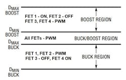
This topology offers a simple solution with an approach that requires neither cumbersome magnetics nor additional control loops. The design takes the form of a synchronous buck or boost, depending on the input voltage. Transitions between modes depend on the duty cycle and are quick and automatic (Fig. 2).
Example #1.: Powering LED from Single Li-ion Cell
As an example, a simple buck-boost converter was designed using the SLG47105 IC and Go Configure software (Figs. 3 through 5). Its purpose is to drive a 3-W LED from a single Li-ion cell. It has the following parameters:
- Input voltage range: (VIN) 2.7 to 4.2 V
- Output voltage: 2.9 to 3.6 V (depending on the LED type)
- Output current range: 650 mA (regulated)
- PWM frequency: 200 kHz
- Overcurrent/short-circuit protection: Internal OCP
Calculated values for buck:
- Rated peak withstand current (IPK): 1.3 A
- Inductance (LMIN): 2 µH
- Filter capacitor (C): 22 µF
Calculated values for boost:
- Min. duty cycle: 10%
- Max. duty cycle: 25%
- Min. inductor size: 1.9 µH
- Peak inductor current: 1.73 A
- Filter capacitor (C): 63 µF
Also, to avoid ACMP oscillation, external hysteresis must be considered (in this case, internal 32-mV hysteresis will be unavailable). To do that, the ACMP0H output must be connected to any available output pin, and from that pin, a 200-kΩ resistor should be connected to Pin 3 (ACMP0H IN-).
The graphs in Figures 11 and 12 show the device’s performance.


Conclusions
Optional section, remove if not required. This section contains any conclusions based on the content of the document.
As can be seen, designing and building buck-boost converters using the HVPAK SLG47105 chip is quite easy. The amount of unused macrocells leaves plenty of room for modifications and adding new features for proposed designs.
For example, a soft-start where a PWM period slowly increases from 0 to the required value reduces a peak startup current, programmable overcurrent protection, multiple output voltages, etc. Also, the HV OUT pins are suitable for driving external MOSFETs, which allows for building a very high-power DC-DC converter.
Nazar Sliunchenko graduated from National University "Lviv Polytechnic" in 2008, studying at the Department of Telecommunications, Radioelectronics & Electronic Engineering. He has more than 15 years of experience in hardware design, including analog and digital devices. Currently, Nazar is managing one of the Technical Documentation departments at Renesas Electronics Corp.
References
GP file https://www.renesas.com/document/scd/cm-358-gp-file
About the Author
Nazar Sliunchenko
Technical Documentation Manager, Renesas Electronics
Nazar Sliunchenko graduated from National University "Lviv Polytechnic" in 2008, studying at the Department of Telecommunications, Radioelectronics & Electronic Engineering. He has more than 15 years of experience in hardware design, including analog and digital devices. Currently, Nazar is managing one of the Technical Documentation departments at Renesas Electronics Corp.
Comment About the Article
To join the conversation, and become an exclusive member of Electronic Design, create an account today!

Leaders relevant to this article: