Hybrid Inverters: A Potential Power Alternative for EVs?


After decades of domination by silicon, silicon carbide (SiC) is replacing it as the gold standard in high-voltage power electronics, including in traction inverters at the heart of electric vehicles (EVs). Besides serving as one of the key building blocks in EVs, the wide-bandgap semiconductor is playing a pivotal role in power inverters for solar, wind, and other renewable-energy systems and for the purposes of data-center power distribution.
Driving the shift is the fact that SiC MOSFETs can reduce switching power losses and squeeze into a smaller space than silicon IGBTs at the same voltage rating. The tradeoff is that they are more expensive than IGBTs. Executives at power electronics companies warn that automakers and other customers are pressuring them to reduce prices for SiC power devices as fast as possible—and, in some cases, even faster than that.
STMicroelectronics is trying to split the difference with a hybrid switch architecture that uses SiC power FETs placed in parallel with its trench-gate field-stop IGBTs to reduce costs without compromising the inverter’s high efficiency. The company is in the early stages of testing the concept, and it is exploring a wide range of other innovations for EV powertrains, too. But the hybrid inverter could present a stop-gap solution as SiC MOSFET prices come down over time.
The company promoted the concept at APEC 2024, where it also presented a galvanically isolated gate driver to be paired with hybrid power stages comprised of both SiC MOSFETs and IGBTs.
SiC: Powering the High-Voltage Future of the EV
A traction inverter is a core building block in EVs, as it converts high DC voltages from the battery pack into AC voltages that control the electric motor’s torque and speed. How efficiently it performs the power conversion directly impacts the EV’s range.

At the heart of the inverter are the power transistors—typically SiC power FETs or IGBTs—that control the flow of current from the high-voltage battery to the EV’s motor. These devices must be protected throughout their operation, so their temperature, voltage, and current must be closely monitored. The MCU in the system is used to supply the pulse-width-modulation (PWM) signals that control the high and low sides of the power inverter.
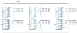
In EVs, the inverter uses three “phases” of power transistors. These are assembled into several power stages driven by the isolated gate driver, which acts as the interface between the MCU and power FET or IGBT. Each power stage is connected to the high-voltage DC bus decoupled by several large capacitors to output the three-phase AC waveform that drives the EV’s motor. The topology of the power stage typically depends on a system’s output power requirements.
In the half-bridge configuration, the phase is assembled out of a pair of power switches. The full-bridge topology, which is preferred for higher power levels of 10 kW to 100 kW or more, is comprised of four power switches. Manipulating such large amounts of power within the space constraints of a modern EV or a data center isn’t easy. In general, IGBTs must be made physically larger to tolerate the higher voltages used by EVs and other power systems.
One of the most valuable properties of SiC is that it can deal with higher breakdown voltages, ranging from several hundred to several thousand volts, than silicon. Since SiC MOSFETs are more robust, they can handle the same amount of voltage as a silicon IGBT in a smaller space.
These chips also have a higher mobility of electrons in the channel—the area under the MOSFET’s gate that sends current from the source to the drain. As a result, they can turn on and turn off significantly faster than IGBTs, saving power. On top of the superior power-handling capabilities, SiC power FETs have higher thermal conductivity than IGBTs, enabling more efficient cooling. They can work safely with higher operating temperatures, too.
However, SiC power FETs cost a premium. These chips lack the massive economies of scale of silicon IGBTs, and they’re more prone to imperfections in the manufacturing process, driving up the prices for non-defective chips.
Integrating SiC and Si Makes Material Difference
But is it possible to integrate SiC MOSFETs and IGBTs to minimize the drawbacks of both?
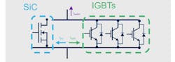
Instead of using the same power device for every facet of the inverter, ST said it’s testing what it calls a hybrid architecture that employs SiC MOSFETs and IGBTs. In its configuration, every phase of the inverter uses a pair of full bridges. Each phase can output up to 10 kW, which equates to 30 kW total power. Inside the full bridge, the transistors are arranged in a 3-to-1 ratio with three IGBTs for every SiC MOSFET. The IGBTs are placed in parallel with the MOSFET to handle larger peak currents.
Importantly, ST said the power transistors are rated for up to 1,200 V. Thus, they can safely handle bus voltages of up to 800 V, which is emerging as the industry’s standard for EV batteries.
But even more important is the switching process for the power stage, which changes depending on the load conditions. At light loads, the SiC power FET is switched on before the IGBTs parallel to it. Since SiC MOSFETs have lower conduction and switching losses than silicon IGBTs, switching them on first boosts the inverter’s power efficiency. This is useful when light load currents are the usual operating mode. For instance, most uninterruptible power supplies (UPS) in the data center run at 20% to 40% of their full load.
The same switching order is used at medium loads to minimize the power losses experienced by the hybrid switch. When the SiC power FET switches on, the voltage traveling through the device drops. The steep drop in the voltage leads to zero voltage switching (ZVS)—also called soft switching—of the IGBT placed in parallel with the SiC MOSFET, according to ST. Thus, most of the switching losses occur in the SiC MOSFET, which is significantly lower than the switching losses of the IGBTs at the same current.
Later in the switching process, the SiC MOSFET in the hybrid power stage is turned off first through hard switching, which subsequently makes it possible to turn off the IGBT using soft switching.
When the current traveling to the load is closer to its peak, the switching order is inverted. The IGBTs are present to share the current with the SiC power FETs, which are prone to permanent damage during short circuits and overcurrent conditions. At high loads, when the current can outrun the safe operating area (SOA) of the SiC MOSFET, the IGBTs are turned on first. To keep switching losses to a minimum, the SiC MOSFET is subsequently turned on and off through soft switching.
By replacing all but one of the SiC MOSFETs in the power stage with IGBTs, the company said the hybrid inverter reduces costs while losing only a fraction of its power efficiency—at least at light loads.
Preliminary tests showed that the hybrid power stage only sacrifices around 0.5% of its power efficiency at light loads versus a power stage based completely on SiC MOSFETs, according to ST. The company said it started focusing on light loads based on the assumption that the inverter spends most of its time under such conditions.
Gate Drivers: The Key to Hybrid Power Inverters
Unlike switching several of the same power transistors placed in parallel, switching a hybrid power device is a more complicated process. Since SiC power MOSFETs have faster switching frequencies than IGBTs and since the switching order changes depending on the load current, the turn-on and turn-off phases for the SiC MOSFET or the IGBT must be delayed very slightly to make sure that the power transistors are switching in sync.
At APEC, ST demoed a single-chip galvanically isolated gate driver that is uniquely designed to drive IGBTs and SiC MOSFETs at the heart of these hybrid switches. The STGAP can control turn-on and turn-off times to make sure the first power transistor that's switched on or off—using hard switching—is fully switched on or off before the other power transistor in the topology is turned on or off using the soft switching process.
The gate driver can independently control the MOSFET and IGBTs to reduce unnecessary power losses and prevent unintended consequences, including short circuits that may permanently damage the power supply.
The STGAP is designed with a dual-output architecture, giving it the ability to output up to 0.6 A of sink and 2.5 A of source current from one of the output pins, while the other pin can deliver 2.4 A of sink and 0.6 A of source. The current used to drive the power FET or IGBT determines how long it takes to turn on and off. The longer it takes to transition between the on and off states—called dead time—the more power it loses in switching the process.
ST said the gate driver is designed to be placed in front of a separate MOSFET that increases the current to control the turn-on and turn-off times of the SiC MOSFETs, which have special requirements for control and driving relative to IGBTs. It also integrates the controller for a separate isolated flyback power supply in the system, making it possible to supply positive and negative voltages to switch the power FET or IGBTs on and off.
The gate driver can be programmed over the SPI bus, giving it the flexibility to be used in everything from traction inverters and EV charging stations to solar inverters or power supplies in data centers.
While the hybrid switch has the potential to be a valuable tool in the power electronics toolbox, it’s likely not a long-term solution. SiC is becoming one of the key building blocks in EV powertrains, as it can contribute to longer range and faster charging times. ST said all-SiC designs will likely remain the long-term preference as economies of scale drive down the cost of SiC power FETs.
Check out more of our coverage of APEC 2024. Also read more articles in the TechXchange: Silicon Carbide (SiC).
About the Author

James Morra
Senior Editor
James Morra is the senior editor for Electronic Design, covering the semiconductor industry and new technology trends, with a focus on power electronics and power management. He also reports on the business behind electrical engineering, including the electronics supply chain. He joined Electronic Design in 2015 and is based in Chicago, Illinois.
Comment About the Article
To join the conversation, and become an exclusive member of Electronic Design, create an account today!

Leaders relevant to this article: