The GaN Advantage in DC-DC Power Converters

What you'll learn:
- How GaN is used in DC-DC power converters.
- Challenges and advantages of using GaN semiconductors.
When designers need high-voltage to low-voltage DC-DC converter designs, both the input and output voltage will usually fall within a wide range (Fig. 1).
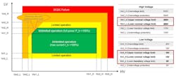
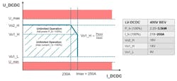
Figure 1 demonstrates the relationship between input voltage and output voltage. We observe that the maximum output voltage is 14 V, while the input voltage drops to 200 V. When the output voltage falls between 14 and 16 V, the converter will be able to output full power with the current derated. Therefore, when the output voltage falls between 9 and 14 V, the converter is able to output the maximum current with power derated (Fig. 2).
The DC-DC converter in the example is capable of operating at 90% efficiency while being able to meet all periodic and random deviation (PARD) performance for space applications.1
Power losses can be reduced by employing advanced power-converter zero-voltage-switching (ZVS) and zero-current-switching (ZCS) topologies. Unfortunately, while the frequency of operation increases, switching losses will reduce efficiency.
>>Download the PDF of this article, and check out the TechXchange for similar articles and videos

The latest benchmark is at 100 V via Infineon’s BSC060N10NS3-G, which has a figure of merit (FOM) of 0.072 Ohm-mm2. Compared to International Rectifier’s IRF100 FOM of 4 Ohm-mm2, it’s close to the theoretical limit for silicon (Si) devices.
Why GaN is Superior Over Si/SiC for Space Applications
GaN transistors hold a number of advantages over silicon and silicon carbide (SiC):
- Lower on-resistance
- Higher switching speed
- Better thermal conductivity
- Smaller physical size
- Lower cost
Advances in GaN HEMT devices have led to a high FOM versus their silicon counterparts. However, they’re both still far from their theoretical limit.6
SiC devices can withstand higher voltages, as high as 1,200 V, while GaN devices withstand lower voltages and power densities. Due to the close to zero switch-off times of GaN devices (high electron mobility along with a dV/dt greater than 100 V/s as compared to the 50 V/s of silicon MOSFETs), they will find homes in very high-frequency applications, bringing high efficiency and performance.
This ideally positive characteristic could prove to be inconvenient, though. If the parasitic capacitances of the component aren’t close to zero, current spikes on the order of tens of amperes can be generated, which may cause problems in the electromagnetic-compatibility test phase.
SiC devices maintain further advantages in the packages used, specifically when adopting TO-247 and TO-220 options, which allows forthe rapid replacement of IGBTs and MOSFETs with the SiC devices. On the other hand, GaN has better results with SMD packages, which are lighter, smaller, and typically relegated to new projects.
Overall, radiation hardening is one of the most crucial requirements of active devices used in space applications. Such devices, like Texas Instruments’ ADC12QJ1600-SP 12-bit, quad-channel, 1.6-GSPS analog-to-digital converter, are available at a 300-krad space-grade quality level.
Summary
Because of the wide bandgap, GaN HEMT devices are far less susceptible to space radiation. That’s because GaN-based crystal structure is said to be radiation hardened by design due to its unique material property. As a result, for the first time in history, power-converter topologies can be designed and operated at megahertz frequency ranges without compromise in power efficiency.
References
1. “Design consideration of low to medium power dc-dc converter using enhancement-mode gallium nitride(e-GaN) HEMT device at MHz switching frequency for satellite payload power supply,” Christopher Parmar, Vasantray Jani, Anupam Kumar, Space Applications Centre, Indian Space Research Organization, Ahmedabad, India 380015; 2021 National Power Electronics Conference (NPEC), IEEE.
2. “TI Designs: TIDA-01634, Multi-MHz GaN Power Stage Reference Design for High Speed DC/DC Converters,” TIDUE47, February 2018.
3. “Active Neutral Point Clamped Resonant DC/DC-Converter in Gallium Nitride Technology,” Tino Kahl, Carsten Kuring, Sibylle Dieckerhoff, Technical University of Berlin; Christopher Fromme, Marvin Tannhäuser, Siemens AG.
4. “Switching Transition Modeling of eGaN HEMT in Power Converters,” Guidong Zhang, Member, IEEE, Yuanhang He, Samson Shenglong Yu Yun Zhang, and Chi K. Tse, Fellow, IEEE; IEEE Transactions on Power Electronics, Vol. 38, No. 4, April 2023.
5. “High-Voltage to Low-Voltage DC-DC Converter Reference Design With GaN HEMT,” Test Report: PMP41078, TIDT403A – August 2024 – Revised December 2024, Texas Instruments.
6. “Wide-bandgap semiconductors: Performance and benefits of GaN versus SiC,” Masoud Beheshti, GaN Applications and Marketing Director, Texas Instruments, ADJ 4Q 2020.
7. “Texas Instruments expands internal manufacturing for Gallium Nitride (GaN) semiconductors, quadrupling capacity,” October 24, 2024.
>>Download the PDF of this article, and check out the TechXchange for similar articles and videos
About the Author

Steve Taranovich
Freelance Technical Writer, Phoenix Information Communication LLC
Steve is a contributing editor to Electronic Design.
Author of the non-fiction “Guardians of the Right Stuff,” a true story of the Apollo program as told by NASA and Grumman Corp. engineers, an astronaut, and technicians.
Experienced Editor-In-Chief of EETimes/Planet Analog and Senior Technical Editor at EDN running the Analog and Power Management Design Centers from 2012 to 2019.
A demonstrated history in electronic circuit design and applications for 40 years, and nine years of technical writing and editing in industry. Skilled in Analog Electronics, Space-related Electronics, Audio, RF & Communications, Power Management, Electrical Engineering, and Integrated Circuits (IC).
1972 to 1988 worked as a circuit design engineer in audio (8 years) and microwave (8 years). Then was Corporate Account Manager/applications engineer for Burr-Brown from 1988 to 2000 when TI purchased Burr-Brown. Worked for TI from 2000 to 2011.
Strong media and communication professional with a BEEE from NYU Engineering in 1972 and an MSEE from Polytechnic University in 1989. Senior Lifetime member of IEEE. Former IEEE Long Island, NY Director of Educational Activities. Eta Kappa Nu EE honor society member since 1970.
Comment About the Article
To join the conversation, and become an exclusive member of Electronic Design, create an account today!

Leaders relevant to this article: