Renesas Pushes GaN into the Kilowatt Class with Next-Gen Power FETs

For decades, silicon has ruled as the undisputed leader in power electronics. But as silicon hits its performance limits, gallium-nitride (GaN) power devices are gaining ground. With faster switching speeds and higher efficiency, GaN is already making a material difference in consumer fast chargers, enabling system-level cost, space, and power savings over silicon. Yet, for all their power-handling properties, lateral high-electron-mobility transistors (HEMTs) based on GaN have been struggling to break into kilowatt-class power designs.
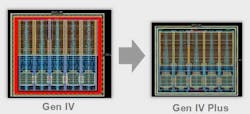
Renesas Electronics is trying to change that with its latest high-voltage GaN power FETs, designed for demanding systems ranging from AI server power supplies and uninterruptible power supplies (UPS) in data centers to EV chargers, inverters, and renewable-energy storage systems. Featuring a 14% reduction in on-resistance, Renesas said the Gen IV Plus family integrates 650-V GaN FETs with a silicon-compatible gate, reducing switching losses while preserving the flexibility and simplicity of silicon FETs.
Available in compact TOLT, TO-247, and TOLL packages, the devices are designed to support power levels ranging from 1 to 10 kW — and even higher with paralleling. The surface-mount packages include bottom-side (TOLL) and top-side (TOLT) thermal conduction paths to reduce heat, allowing for easier paralleling when higher conduction currents are needed. The TO-247 package supports even higher thermal capabilities to scale up to higher power levels.
“Renesas is doubling down on GaN,” said Primit Parikh, VP of the company’s GaN power business and a co-founder of Transphorm, a power semiconductor startup that it acquired in 2024. He noted that Renesas has also paused development of silicon-carbide (SiC) devices and IGBTs to focus on expanding its footprint in fast-growing markets such as data centers, where GaN enables more compact and efficient power conversion. He added, “GaN will eventually replace a lot of applications happening with silicon and silicon carbide devices.”
Parikh said the new strategy is all about building out a more complete — and competitive — roadmap of GaN power FETs, pushing the wide-bandgap semiconductor to power levels ranging from tens of watts to over 100 kW with paralleling. The company is now investing in what he calls the “GaN ecosystem — a product-based offering. By a GaN ecosystem, we mean GaN devices, drivers, controllers, ICs, and solutions.”
Renesas is also shifting production from 150-mm to 200-mm GaN-on-silicon wafers to reduce costs. “The cost of GaN is becoming very competitive, and manufacturing is also scaling to larger diameter wafers,” noted Parikh.
The Differences Between D-Mode and E-Mode Power GaN
The new Gen IV Plus family leverages the company’s SuperGaN technology, a robust depletion-mode (d-mode), normally-off architecture developed by Transphorm, along with Renesas’ easy-to-cool packaging.
Unlike a silicon MOSFET, d-mode devices are switched “on” by default, enabling current to flow from source to drain without any gate voltage. As a result, the power transistor must be intentionally turned off by applying a negative voltage to the gate of the device.
To make sure that the power device remains switched off, a separate silicon FET is placed inside the package to control the gate voltage of the GaN. The MOSFET interfaces with the gate driver in the power supply, switching the GaN on and off every cycle.
>>Check out these TechXchanges for similar articles and videos


This contrasts with more widely used enhancement-mode or e-mode devices, which resemble standard silicon MOSFETs. In e-mode, the power transistor is normally “off” and turns on with a positive gate voltage. These devices incorporate a small sliver of GaN — also called p-type doped GaN — directly under the device’s gate to keep the transistor turned off.
While these FETs are relatively easy to drive, they can add a lot of complexity to the manufacturing process that can take a toll on performance at high voltages, said Parikh.
While e-mode continues to be the gold standard for low-voltage GaN, Renesas explained that d-mode has potential for high-voltage, multi-kilowatt power systems, where performance, efficiency, and cooling are pain points.
One of the tradeoffs with e-mode devices is that saturation current (IDsat) could reduce by approximately 50% as temperature increases. The IDsat refers to the maximum current that flows from the drain to the source of a power transistor when it’s fully turned on. Parikh said its d-mode devices can supply significantly more current than e-mode, even under the high operating temperatures typical at kilowatt power levels. “That means you can get more power from a smaller chip at higher efficiency.”
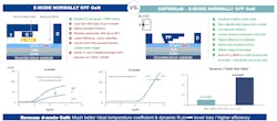
Another tradeoff stems from a characteristic of GaN called “dynamic on-resistance,” which means the on-resistance of the device depends on the breakdown voltage of the device when it’s conducting current. A higher voltage rating (such as 650 V) means a higher on-resistance, which ultimately translates to higher power losses. Renesas said its d-mode devices aren’t as influenced by dynamic on-resistance as e-mode.
On top of that, the company said the d-mode architecture can handle higher threshold voltages—up to 4 V—which is currently impossible with e-mode. As a result, according to Renesas, customers can avoid using a negative gate-drive voltage, which is frequently required with e-mode devices to improve noise immunity. The ability to handle higher voltages also lowers the risk of voltage overshoots, enhancing its reliability when dealing with kilowatts worth of power. GaN power FETs operating in e-mode have typical thresholds of 1.5 to 1.7 V.
Renesas said SuperGaN also stands out for its flexibility. In many cases, special high-performance gate-driver ICs are required to stay ahead of the faster switching frequencies of e-mode devices. By using a silicon MOSFET on the front end of the device, its GaN power FETs work with standard, off-the-shelf gate drivers, and the gate-drive voltages can be configured to a customer’s requirements. The broad compatibility helps simplify design and ease the integration of GaN into high-density power systems.
The final advantage is robustness. While e-mode devices can handle a relatively limited gate voltage range of between 6 and 8 V, the new d-mode devices will operate at up to ±18 V. As a result, the SuperGaN technology can tolerate more noise than most other GaN power devices. That helps prevent the unintended turn-on of the power transistor due to transient voltages at the device’s gate, often caused by noise.
By mitigating gate overstress risks, Renesas said it can deliver GaN devices in traditional power packages such as the TO-247 and TO-220 without additional protection, enabling drop-in upgrades for existing high-power designs.
By the Numbers: High-Voltage GaN Power FETs from Renesas
While based on the same SuperGaN technology as its Gen IV platform, Renesas made a wide range of improvements to chip design and the process technology to push the performance boundaries of GaN.
One of the main characteristics of a GaN power switch is its high mobility of electrons in the channel, which runs under the device’s gate and through which current flows between the source and the drain. That gives it much higher switching frequencies than silicon, enabling not only more efficient power conversion, but also a reduction in the size of the magnetics and passives in the system, saving costs at a system level.
Based on a 14% smaller die than the Gen IV technology, Renesas said the Gen IV Plus reduces the on-resistance by the same percentage to 30 mΩ, reducing switching power losses and the associated heat.
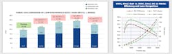
It also upped the switching performance of the power FETs, including up to a 50% improvement in the on-resistance times the gate charge (Qg)—what Parikh termed the main “input figure of merit.” The Qg, which is the total charge required to turn the power transistor on and off, is one of the keys to determining the device’s power losses in high-frequency power supplies.
Renesas said Gen IV Plus also brings a 20% improvement in resistance times output capacitance (Qoss) — what Parikh referred to as the main “output figure of merit.”
By minimizing power losses with lower gate charge, lower output capacitance, and lower dynamic resistance and maximizing robustness in real-world conditions, Gen IV Plus can compete with more than just silicon in power electronics—but also SiC, according to the company.
While GaN dominates at higher frequencies, it’s widely held that SiC outperforms GaN at more moderate switching speeds. But Parikh explained that the material properties of GaN, including its higher electron mobility and transconductance, potentially put it ahead over the entire frequency range. “Higher frequencies are required as power systems need to get compact, and so everyone is looking at frequencies of more than 500 kHz and GaN itself is capable of even higher in the 1-MHz range.”
To support this claim, Renesas said it tested the new GaN FETs at moderate frequencies around 100 kHz in a 3.6-kW server power-supply unit. The GaN devices showed 10% to 30% lower power losses compared to SiC MOSFETs. SiC is becoming the standard in the half-bridge boost power-factor-correction (PFC) stages in AC-DC server power supplies—a key building block of data center power architectures. Parikh said GaN beats SiC at moderate frequencies, and the gap widens at higher rates.
“GaN delivers 10 to 30% lower losses, which is very significant at 4-, 5-, 6-, 10-kilowatt levels,” said Parikh, “and you can only imagine what a 10 to 30% loss reduction can help accomplish when you start scaling up to a megawatt of data center rack power.”
The Ecosystem: Gate Drivers, Controllers, and Protection for GaN
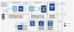
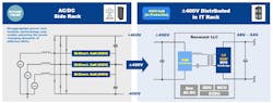
Renesas said the 650-V GaN FETs are already in production, targeting data center power supplies ranging from 1.2 to 7.5 kW. The devices are being deployed in high-efficiency topologies, including totem-pole PFC AC-DC stages and LLC DC-DC converters. Looking ahead, Renesas is preparing to push its high-voltage GaN technology into 800- and 400-V high-voltage DC (HVDC) architectures for data center and industrial power systems.
The Gen IV Plus products have also been adopted in other high-power markets such as inverters for renewable energy and high-performance gaming PC power supplies, where heat is one of the main design constraints.
As part of its broader ambitions in GaN, Renesas is developing what it calls a “GaN ecosystem,” where it will tightly integrate its GaN power devices with gate drivers, controllers, and protection circuits in the same package or on the PCB. This system-level strategy is aimed at moving GaN out of consumer fast chargers and into higher-power, thermally demanding environments such as onboard chargers (OBCs) and traction inverters in EVs.
“Whether used as standalone FETs or integrated into complete system solution designs with Renesas controllers or drivers, these devices will provide a clear path to designing products with higher power density, reduced footprint, and better efficiency at a lower total system cost,” said Parikh.
Renesas is also expanding its GaN development into the low-voltage domain, giving it the ability to cover high voltages of more than 600 V with d-mode and voltages of under 200 V with e-mode. GaN is gaining ground for synchronous rectification in server power supplies and 48- to 12-V DC-DC converters in servers. By supplying both types of power FETs, the company said it can fill in more of the blanks in current and future rack architectures.
Further down the line, Renesas plans to expand its portfolio with 650-V bidirectional GaN power FETs for data centers. These devices are targeted at disaggregated power architectures proposed by hyperscalers Google, Meta, and Microsoft.
“We have a rich roadmap of GaN devices,” said Parikh.
>>Check out these TechXchanges for similar articles and videos
About the Author

James Morra
Senior Editor
James Morra is the senior editor for Electronic Design, covering the semiconductor industry and new technology trends, with a focus on power electronics and power management. He also reports on the business behind electrical engineering, including the electronics supply chain. He joined Electronic Design in 2015 and is based in Chicago, Illinois.
Comment About the Article
To join the conversation, and become an exclusive member of Electronic Design, create an account today!

Leaders relevant to this article: