Scaling AI Data Center Power Delivery with Si, SiC, and GaN

This article is part of an Electronic Design special report.

Large language models (LLMs) and other neural networks draw substantial power when processing complex artificial-intelligence (AI) and machine-learning (ML) workloads. Designed for traditional server configurations, conventional power-supply units (PSUs) can’t efficiently keep pace with the demands of GPU-based AI accelerators. To meet evolving workload requirements, data center operators need power-delivery systems that scale within existing thermal and physical limits—without increasing cost, power use, or cooling overhead.
The PSU is the power backbone of the data center, converting high-voltage AC power from the grid into the lower-voltage DC used by all of the components within the server rack. To deliver higher output and improved efficiency while minimizing losses and managing heat, many engineers are leveraging new architectures that combine silicon with wide-bandgap (WBG) semiconductor materials such as silicon carbide (SiC) and gallium nitride (GaN), which improve switching performance and thermal stability under heavy AI workloads.
This article outlines the complementary roles of all three power semiconductors, focusing on how these technologies have been integrated over several generations of Infineon’s PSU reference designs, ranging from 3 to 12 kW.
Silicon: Can It Meet the Power Demands of AI?
While silicon has long been the foundation of power electronics, its physical limitations are increasingly apparent in high-performance, high-density applications such as AI server racks and other data center infrastructure.
High-performance GPUs now operate at up to 1,000 W each, with projections reaching 2,000 W and beyond by the end of the decade—comparable to the total draw of a legacy server just a few years ago. As AI hardware and applications continue to scale, PSU power ratings must increase from typical levels of around 800 W to 5.5 kW and higher. Infineon estimates that data centers could consume up to 7% of global electricity by 2030—roughly equivalent to India’s current national energy use.
This surge in power demand—combined with grid constraints such as limited substation capacity, transmission bottlenecks, and variable renewable generation—highlights the urgency of deploying more efficient power systems in data centers. Rather than absorbing the steep cost of new construction or shifting the AC-DC power supplies into separate racks, many operators are opting to increase power density while staying with existing rack footprints.
As demand grows for higher voltages, faster switching frequencies, and greater power density, conventional silicon-based devices—such as metal-oxide-semiconductor field-effect transistors (MOSFETs)—are reaching their performance and efficiency ceiling.
To support the requirements of compute-intensive AI and ML workloads, the latest PSUs leverage WBG semiconductors such as SiC and GaN with lower on-resistance (RDS(on)), higher switching speeds, and reduced losses. While these materials have superior power-handling properties, they’re also edging closer to silicon in cost. As mass production scales up and design processes mature, prices are set to drop substantially. These trends position SiC and GaN power devices as practical complements to silicon in the design of dense, efficient, and thermally optimized PSUs for the AI era.

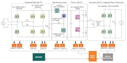
But there are tradeoffs with all three technologies when it comes to efficiency, power density, and cost. To understand where each technology fits into the present and future landscape of AI power delivery, we’ll take a closer look at how Infineon’s power-supply designs have evolved to address the ever-increasing power demands of AI data centers. Solutions scale from 3 to 12 kW, and output voltages reach up to 50 V DC to support busbar distribution in AI server racks (Figure 1).
These designs deliver efficiencies of up to 98%, meet strict hold-up time requirements, and achieve power densities as high as 100 W/in³. Several of them align with Open Compute Project (OCP) ORv3 standards and support rack-level loads of up to 250 kW and beyond.
The 3-kW PSU: Benefits of SiC-Based Power Switching
The first-generation AI PSU features a front-end AC-DC bridgeless totem-pole power-factor-correction (PFC) converter followed by a back-end, isolated, half-bridge, series-parallel resonant LLC converter. The 3-kW PSU leverages CoolSiC MOSFETs and CoolMOS switches to achieve a peak efficiency of 97.5% with an internal DC fan and 97.4% without one. Its compact form factor—73.5 × 520 × 40 mm—yields a power density of approximately 32 W/in³.
In the OCP ORv3 architecture, each power “shelf” in the server rack houses several PSUs. While the input for the power shelf is three-phase AC ranging from 400 to 480 V, the input for each PSU is single-phase AC from 230 to 277 V. The PSU outputs a tightly regulated DC voltage, such as 48 or 50 V, to the busbar that runs down the server rack, feeding power into the AI servers and the battery backup units (BBUs) located under the rack.
At 50% load, the main losses in the totem-pole PFC stage originate from the half-bridge boosting switches, which operate predominantly in hard commutation. To address this, the design uses 650-V CoolSiC MOSFETs in 4-pin packages, which feature low parasitic capacitances to support high switching frequencies. In the slow leg of the totem pole, a silicon CoolMOS replaces the diode rectifier to enable synchronous rectification (SR), which reduces conduction losses.
SiC MOSFETs excel in high-current, high-voltage applications. They have minimal reverse-recovery charge (Qrr) and a more temperature-stable RDS(on) than silicon MOSFETs due to the higher thermal conductivity of SiC. They optimize performance in both soft- and hard-switching topologies. In the totem-pole PFC stage, which operates in a hard-switched, continuous-conduction mode (CCM) when managing kilowatts of power, SiC supports higher switching frequencies, reduced commutation losses, and improved overall efficiency.
In the LLC converter stage, transformer losses are a primary contributor, along with significant switching and driving losses. To optimize performance and power density, the converter operates at a relatively low resonant frequency of 93 kHz. Silicon CoolMOS devices offer the best cost-performance ratio for this frequency range and board size.
Complementary Properties of Silicon, SiC, and GaN
The second generation is a high-frequency, high-density 3.3-kW PSU that leverages all three power switching technologies to maximize the efficiency, power density, and overall cost of the system. The front-end AC-DC converter features a two-phase, interleaved, bridgeless totem-pole PFC with CoolSiC, while the back-end isolated DC-DC stage implements a 500-kHz, GaN-based, half-bridge LLC converter with full-bridge rectification.
The PFC stage comprises a pair of interleaved totem poles featuring a total of four 650-V CoolSiC MOSFETs for the fast legs. EMI performance is also improved through careful circuit refinement. Notably, substantial reductions in both line and neutral positive-peak EMI are achieved by optimizing the zero-crossing sequence in the PFC and using a total of four 600-V CoolMOS SJ MOSFETs in the slow leg of the bridgeless totem-pole PFC.
Compared to the first-generation 3-kW PSU, the 3.3-kW design operates at a significantly higher resonant switching frequency of 500 kHz. To support this, the LLC stage uses a total of four CoolGaN devices in place of CoolMOS, optimizing efficiency and power density at high switching frequency.
GaN power devices thrive in situations where high-frequency switching is important. Their lack of a body diode results in zero Qrr, which minimizes switching losses. This enables shorter dead times, thus reducing unnecessary conduction losses. GaN also features very low output capacitor charge (Qoss), which helps facilitate zero voltage switching (ZVS), especially in soft-switching LLC converters. It can also enable more efficient operation in hard-switched, half-bridge topologies such as totem-pole PFC.
The design also features Kelvin source connections. The 80-V OptiMOS switches used for synchronous rectification in the LCC converter have dedicated gate drivers, further minimizing losses and enabling accurate, high switching frequencies.
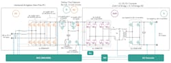
The design incorporates a “baby-boost” converter in between the AC-DC rectifier and the DC-DC converter stages to meet the 10 milliseconds of hold-up time required in server applications—without significantly increasing bulk capacitance. This addition reduces the capacitor volume, contributing to higher overall power density (Fig. 2).
The PSU delivers a peak efficiency of 97.4% without internal cooling fans and a power density of 98 W/in³, based on compact outer dimensions of 72 × 192 × 40 mm.
The 8-kW PSU: More SiC, More GaN, and More Silicon Power Switching
As high-performance AI chips drive up power-per-rack specifications in data centers to more than 100 kW, supplying more power in a smaller space is becoming critical. Infineon introduced a single-phase 8-kW PSU reference board to manage these mounting power demands. This design builds on the architecture of the 3.3-kW design and scales it up to higher power levels, leveraging all three semiconductor technologies to an even greater degree to optimize performance, size, and cost.
The front end comprises a bridgeless interleaved totem-pole PFC converter that regulates the intermediate high-voltage bulk. Due to elevated current stresses, all of the power switches in the PFC stage—in both the fast and slow legs—are based on SiC. The interleaved totem poles each have a pair of SiC MOSFETs placed in parallel to achieve a lower equivalent RDS(on) and reduce conduction losses. The fast legs feature a total of eight 650-V, 40-mΩ SiC MOSFETs, while the slow legs leverage four 650-V, 10-mΩ SiC MOSFETs.
The back-end stage is an isolated LLC converter that regulates the 50-V DC nominal output. The primary side of the isolated DC-DC converter is implemented with eight 650-V GaN power devices to reduce driving losses and switching losses at high frequencies. The bridge is located on a separate daughter card and drives a pair of high-frequency, series-connected transformers. The synchronous rectifier on the secondary side of the DC-DC converter is based on 80-V OptiMOS silicon MOSFETs.
To meet server hold-up time requirements, the design includes a more advanced baby-boost converter to support a maximum 20-ms hold-up time at 100% of output power while the PSU is losing input AC voltage. During normal operation, the auxiliary boost converter—also referred to as the hold-up time extension circuit—is idle and is bypassed by a 600-V CoolMOS SJ MOSFET.
Overall, the 8-kW reference design achieves a 97.5% peak efficiency and maintains a minimum efficiency of 96.5% across the 30% to 100% load range at 230-V AC input, including fan power consumption. Its outer dimensions of 73.5 × 450 × 40 mm correspond to a power density of 100 W/in³—twice that of the OCP ORv3 specification. Additional efficiency is achieved through digital control, integrated magnetics, and optimized thermal design.
The 12-kW PSU: From Single- to Three-Level Converter Topologies
The next stage in the roadmap is a single-phase 12-kW PSU reference designthat reflects the latest advances in high-efficiency power conversion for data centers. The design will feature a modular architecture composed of a pair of 6-kW modules, each with a 1/2 U form factor, enabling them to be combined for scalable output power. This modularity bolsters light-load efficiency, simplifies manufacturing, and improves power density.
The PSU will adopt a fully three-level conversion topology in both the PFC and the LLC converter stages, enabling operation at higher input voltages by leveraging semiconductor switches with lower voltage ratings.
The two-level totem-pole PFC in the previous generation will be replaced by a three-level flying-cap totem-pole PFC based on 400-V CoolSiC MOSFETs. One of the benefits of a multi-level topology is that it can effectively multiply the switching frequency of the power MOSFETs by the number of levels minus one. As a result, the three-level flying cap topology can reduce the PFC choke size and improve EMI. That not only improves power density, but it also helps thermal performance by enabling more efficient airflow from the internal fan.
Unlike traditional LLC-based topologies, the DC-DC stage operates as a DC transformer, offering faster dynamic response to accommodate rapid load changes from GPUs while maximizing efficiency. These GPUs can require huge amounts of current when leaping to full power, resulting in large load transients. To limit voltage overshoot and undershoot, the DC-DC stage must be able to adjust the output voltage as fast as possible. The three-phase LLC converter will use WBG semiconductors to run at faster switching frequencies, increasing the control-loop bandwidth and giving it more dynamic control of the output voltage.
More advanced digital controllers are also used to stay on top of these power spikes, which can result in load transients as fast as 2.5 A per microsecond at the PSU level. In the 12-kW power supply, digital control is managed through Infineon’s PSoC 3 and XMC microcontrollers. These MCUs provide real-time monitoring, predictive maintenance, and remote diagnostics—further improving system uptime and operational reliability.
A power pulsation buffer circuit takes the place of the baby-boost converter in the other designs. It smooths out input current from the grid and reduces the bulk capacitance required to meet hold-up time specifications.
Advanced thermal management and high-performance components enable the 12-kW PSU to achieve a peak efficiency of 97.5% and a power density of more than 100 W/in³, with outer dimensions of 69 × 720 × 40 mm.
Transforming PSU Design with Wide-Bandgap Devices
These PSU reference designs represent a clear upgrade path from 3 kW and 3.3 kW to next-generation 8- and 12-kW designs, supporting both greenfield deployments and the replacement of legacy AI power supplies.
However, they also reflect a broader industry shift toward digitally controlled, high-efficiency power systems designed for next-gen AI workloads. By strategically combining CoolMOS, CoolSiC, and CoolGaN devices in power topologies that are being reshaped and refined over time, these solutions optimize thermal management and system reliability at scale. As data centers push for greater density, energy efficiency, and carbon reduction, Infineon’s reference designs offer a foundation for high-performance, sustainable power delivery.
Remove more articles in the special report
About the Author
Justin Chou
Application Marketing Director, Infineon Technologies
Comment About the Article
To join the conversation, and become an exclusive member of Electronic Design, create an account today!

Leaders relevant to this article: