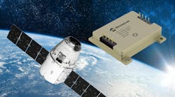
Space-Rated MOSFET Family Adds First Rad-Tolerant P-Channel Device

P-channel power MOSFETs are now part of Infineon Technologies’ mix of radiation-tolerant MOSFETs for low-Earth-orbit (LEO) systems. Included in the company’s expanding portfolio of devices for “NewSpace” applications, the new 60-V P-channel MOSFET provides a cost-optimized, radiation-tolerant solution for designs using smaller and lighter-weight components with radiation performance suitable for missions lasting two to five years.
The P-channel MOSFET complements the already available 60- and 150-V N-channel devices, all offered in plastic packaging, which is lower in cost than the traditional hermetic packaging used in rad-hardened devices. It can also be produced in higher volumes using standard manufacturing practices.
The rad-tolerant discretes, space-qualified to the requirements of the AEC-Q101 standard, are rated for single event effects (SEE) at 46 MeV∙cm2/mg linear energy transfer (LET) and a total ionizing dose (TID) of 30 to 50 krad (Si).
Next in This Edition of PowerBites
More PowerBites


About the Author

Lee Goldberg
Contributing Editor
Lee Goldberg is a self-identified “Recovering Engineer,” Maker/Hacker, Green-Tech Maven, Aviator, Gadfly, and Geek Dad. He spent the first 18 years of his career helping design microprocessors, embedded systems, renewable energy applications, and the occasional interplanetary spacecraft. After trading his ‘scope and soldering iron for a keyboard and a second career as a tech journalist, he’s spent the next two decades at several print and online engineering publications.
Lee’s current focus is power electronics, especially the technologies involved with energy efficiency, energy management, and renewable energy. This dovetails with his coverage of sustainable technologies and various environmental and social issues within the engineering community that he began in 1996. Lee also covers 3D printers, open-source hardware, and other Maker/Hacker technologies.
Lee holds a BSEE in Electrical Engineering from Thomas Edison College, and participated in a colloquium on technology, society, and the environment at Goddard College’s Institute for Social Ecology. His book, “Green Electronics/Green Bottom Line - A Commonsense Guide To Environmentally Responsible Engineering and Management,” was published by Newnes Press.
Lee, his wife Catherine, and his daughter Anwyn currently reside in the outskirts of Princeton N.J., where they masquerade as a typical suburban family.
Lee also writes the regular PowerBites series.
Comment About the Article
To join the conversation, and become an exclusive member of Electronic Design, create an account today!

Leaders relevant to this article: