The Many Sintering Options to Boost Power Density
Key Highlights
- The role of sintering in high-density power electronics.
- When is sintering the best choice?
- Promising developments with sintering technology.

Doing more with less and, of course, packing more power into a smaller form factor means taking advantage of any applicable technology. One of those technologies is sintering, a well-established alternative to soldering. Sintering can add complexity but also solves many problems.
Sintering plays a critical role in enabling high-density power electronics. It provides a robust, thermally conductive, and reliable method for attaching power semiconductor devices (e.g., SiC or GaN chips) to substrates, leadframes, or heatsinks — especially in demanding applications where soldering reaches its limits (e.g., operating temperatures that can approach the melt point of some solders).
Sintering in this context typically refers to pressure-assisted or pressure-less bonding of nanosilver or other metal particles at temperatures below their melting point. The process forms a dense metallic bond between surfaces through atomic diffusion, creating a joint with high thermal and electrical conductivity and excellent mechanical strength.
>>Download the PDF of this article

What is the Role of Sintering in High-Density Power Electronics?
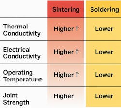
- Improved thermal conductivity: Sintered silver has a thermal conductivity of ~200 to 250 W/m·K, far exceeding typical solders (~50 W/m·K). This helps dissipate heat more effectively from high-power chips, supporting higher power density and smaller form factors.
- High reliability and strength: Sintered joints are void-free and crack-resistant, offering better fatigue performance under thermal cycling and vibration. Likewise, sintering offers excellent electromigration and corrosion resistance, ideal for harsh environments (EVs, aerospace, renewables).
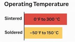
- High-temperature operation: Sintering materials can withstand operating temperatures >250°C, well beyond lead-free solder limit. This is essential for wide-bandgap semiconductors like SiC and GaN, which operate at higher junction temperatures.
When is Sintering the Best Choice?
Sintering is preferred when:
- Power density is high, and heat removal is critical.
- Operating temperatures exceed 200°C (e.g., SiC inverters, EV traction systems).
- Reliability under thermal cycling is a top priority.
- Conventional solder joints are failure-prone, especially under high current or vibration.
- A long operational life (20+ years) is required in mission-critical systems.
Tradeoffs
- Cost: Sintering (especially with silver) is more expensive than soldering.
- Processing complexity: May require pressure, inert atmosphere, or tight process control.
- Equipment: Specialized sintering equipment may be needed for volume production.
Promising Developments with Sintering Technology
Recent and emerging developments in sintering for high-density power electronics address key challenges — cost, scalability, and performance — while unlocking new possibilities for compact, high-reliability systems. Here are some of the most promising innovations:
Low-Temperature, Pressure-less Sintering
New silver pastes and nanoformulations allow sintering at < 200°C without the need for external pressure. This reduces stress on sensitive substrates (e.g., ceramics, polymer hybrids) and enables co-sintering of multiple layers or dies simultaneously. It’s well-suited for automated, high-throughput assembly lines.
Copper Sintering (Ag Alternative)
Copper nanoparticle sintering is emerging as a low-cost alternative to silver, offering comparable thermal/electrical conductivity. This technology requires oxygen-free processing or surface treatments to prevent oxidation. It’s generally suitable for applications where cost constraints or Ag migration are concerns (e.g., automotive, consumer power electronics).
Hybrid Sintering Materials
The development of composite sintering pastes (e.g., Ag-Cu, Ag-graphene, Ag-Sn) combines the strengths of multiple materials that are tuned to optimize thermal expansion, reduce voids, and enhance joint ductility for improved shock/strain resistance. This offers promise for ruggedized electronics, such as aerospace and defense systems.
In-Situ Monitoring and AI-Based Control
The integration of real-time sensing (temperature, pressure, resistance) into sintering platforms can make sintering more practical. AI/ML-driven process optimization enables predictive quality control, reducing defects and increasing yield. This can be particularly valuable in multichip power modules and advanced packaging (e.g., stacked dies).
3D Sintered Interconnects and Printed Power Structures
Additive manufacturing of 3D sintered metal features (vias, bumps, and interconnects) for high-current, high-density modules supports vertical power-module architectures and advanced cooling strategies (e.g., embedded microchannels). It can enable co-packaging of power, logic, and passive elements in ultra-compact formats.
Enhanced Heat-Dissipation Substrates
Sintering is being combined with diamond, graphene, or aluminum-nitride (AlN) substrates to create ultra-high-performance thermal stacks. This can boost heat-flux management in devices like SiC inverters and EV fast chargers. Tailored interfaces using gradient sintered layers reduce thermal expansion mismatch and delamination risk.
Conclusion
Sintering can be a key enabler of high-reliability, high-temperature, high-density power modules. It’s increasingly adopted in EVs, aerospace, and renewable-energy converters, where performance and longevity justify the added complexity and cost.
References
“A Hybrid Pressureless Silver Sintering Technology for High-Power Density Electronics”
“A Hybrid Sintering Technology for High-power Density Devices Used in Aerospace Applications”
>>Download the PDF of this article
About the Author

Alan Earls
Contributing Editor
Comment About the Article
To join the conversation, and become an exclusive member of Electronic Design, create an account today!

Leaders relevant to this article: