Inside a Smart Portable Power Bank with Multi-Source Charging
What you'll learn:
- The building blocks of a smart power bank that can operate from different input power sources, including solar cells, adapters, and batteries.
- The importance of intelligent power-path management that leads to dependable backup power for smartphones and other USB-based devices.
- The differences between a stacked and a single-board design and the impact on efficiency, complexity, and BOM cost.
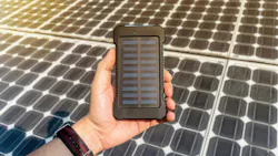
As portable electronics become more power-hungry, power banks are evolving from passive battery packs into intelligent energy-management systems that can offer dependable backup power. These devices must do more than recharge smartphones, tablets, and other USB-powered devices. They also need to run on different input power sources, manage battery charging under changing conditions, and deliver power to connected loads efficiently and reliably.
To meet those demands, we developed a smart power bank charger that started out as a modular proof-of-concept using stacked evaluation boards. The prototype validated the system’s architecture, but the stacked approach came with penalties in size and complexity and caused excess power loss. We later consolidated the power bank into a fully integrated single-board solution that combines all major power-management functions into a smaller and more commercially practical platform.
The all-in-one design can operate from a range of input sources — including solar cells, lithium-ion (Li-ion) batteries, and DC adapters — while using intelligent power-path management to automatically balance power delivery between the load and battery without sacrificing performance.
This article traces the evolution from the early multi-board prototype to the final single-board design, digging into the details of the system architecture, key design considerations, and performance gains through integration.
The Building Blocks of a Smart Power Bank
In this design, a compact and streamlined architecture was developed to support dual wide-range input voltages — namely, from a solar panel and AC-DC adapter. Power input is intelligently managed using the LTC4416 power-path controller in conjunction with the LTC4162 power-path buck charger. This configuration enables efficient charging of various Li-ion batteries up to 4S1P stack battery configurations.
As illustrated in Figure 1, the system contains a buck-boost switching regulator, LTC3115-1. It dynamically regulates the output voltage to the load and ensures a constant maximum output of 5 V and 2 A, as the LTC4162 monitors the battery’s charge level.
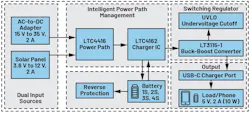
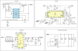
The three main parts of the smart power bank were all selected to improve system efficiency, minimize power loss, reduce PCB layout area, and reduce overall cost. The full schematic is shown in Figure 2.
Dual Input Power Sources
To switch between dual input power sources, a simple OR-gate configuration can be used. However, this approach introduces significant power loss since it depends on diodes, which experience inherent forward voltage drop even when using low-drop Schottky diodes. The LTC4416 can be used as an alternative, enabling seamless switching between two sources with a very low voltage drop, thus reducing power loss.
By controlling the external p-channel MOSFETs to emulate ideal diodes, this device significantly reduces conduction losses, thereby improving overall system efficiency and reliability. The LTC4416 operates in six different modes. Each mode of operation depends on the configuration of the E1 and E2 input pins, as stated in the datasheet.
In this setup, the selected mode is: V1 is greater than V2, where E1 is set to Sense and E2 is set to 0. This means that the chip gives priority to the V1 power source. Using this mode of operation, the IC is configured in such a way that V1 is prioritized to accept a wide input voltage range of 15 to 35 V DC while the V2 power supply is a solar-panel source, acting as a secondary voltage (3.6 to 15 V). When V1 is greater than or equal to 15 V, E1 enables the V1 source to be the primary voltage supply and switches off the V2 supply since V1 is greater than V2.
>>Download the PDF of this article
 dreamstime_dmitriimelnikov_114544075
When V1 drops to 13.4 V, V2 becomes the main power supply while V1 is disconnected from the output. Provided that the voltage from the solar panel is within 3.6 to 15 V, V2 will continue to supply power to the output load until V1 is restored. The restoration point of V1 is set to 15 V (Fig. 2, again).
The fail and restoration point of V1 can be modified by changing the resistor values of R1, R2, and R3 in Figure 2. This can be done by using the formula from the data sheet as given:


Once V1 has been identified, V2 can be selected to guarantee the best configuration. If V1 fails or becomes unavailable, the system automatically switches to V2 to maintain the power supply until the restoration point is reached, as long as V1 > V2. Since the output supply follows the higher voltage source, restoration will not happen if V2 > V1.
Intelligent Power-Path Management
In power banks and other devices that require simultaneous discharging and charging of the battery, implementing power-path charging is an ideal solution. This approach helps extend both the battery’s runtime and its overall lifecycle by efficiently managing power distribution between the system and the battery.
In this case, the system intelligently manages the power input by selecting from three sources: the AC-DC adapter, the solar panel, or the battery. The AC-DC adapter or solar panel is primarily used to charge the battery.
If the AC-DC adapter fails and the solar-panel voltage drops below the minimum value, the system automatically switches to the charged backup battery to supply power to the load. The output from the LTC4416 power path feeds into the LTC4162-L, which supports input voltages up to a maximum of 35 V.
The LTC4162-L supports immediate operation even with a discharged or absent battery. It features integrated maximum power point tracking (MPPT) to enhance solar energy conversion efficiency.
When the sun is shining, the solar panel operates in two regions: low impedance at constant voltage and high impedance at constant current. This behavior ensures that the device’s control loop remains stable when operating at lower impedance (for example, the higher voltage region).
However, as the IC uses input voltage to find the MPPT, the solar panel voltage drops due to higher impedance (for example, the lower voltage region), which makes the control loop become unstable. In the design, the solar-panel input operates at high impedance (<12 V).
To address this, the R-C network (R4 and C1), illustrated in Figure 2, is used to correct the instability of the control loop, particularly in partly cloudy or under varying sunlight conditions. For low-wattage solar panels, a higher capacitance value for C1 (ranging from 100 to 1000 µF) is recommended to ensure robust performance of the MPPT.
Backup Lithium-Ion Battery
The LTC4162 battery charger supports configurations of up to eight series-connected (8S) lithium-ion (Li-ion) cells and has multiple variants optimized for different battery chemistries: LTC4162-L for lithium-ion, LTC4162-F for lithium iron phosphate (LiFePO), and LTC4162-S for lead-acid batteries. In this design, up to 4S configurations (1S power through 4S) of stacked Li-ion cells are supported, as shown in Table 1.
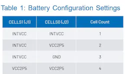
This configuration is defined using the CELLS1 and CELLS0 pins, following the mapping guidelines provided in Table 1.
Switching Regulator
The output of the LTC4162-L is then regulated via a synchronous buck-boost switching regulator. The LTC3115-1 is a high-efficiency, monolithic, synchronous buck-boost DC-DC converter designed for applications requiring a wide input voltage range and low noise.
The switching regulator operates from 2.7 to 40 V and can deliver up to 2 A continuous current. It also features programmable output voltage, seamless transition between buck and boost modes, and robust protection features that are all key for industrial-grade, battery-powered applications.
The LTC3115-1 fits into the smart power bank due to its high efficiency and low-noise operation. The converter can supply up to 2 A when the input voltage exceeds 6 V and 1 A when voltages are above 3.6 V, giving it the flexibility to be used under varying power conditions. For all battery configurations (1S, 2S, 3S, 4S), an undervoltage lockout (UVLO) was configured via the connector (J5), as shown in Figure 2.
USB Type-C Output
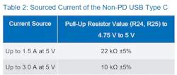
The output was configured with a USB Type-C in non-power delivery (PD) mode to charge any portable devices that require a regulated 5-V output with up to 2-A current. Table 2 outlines the different resistor values for different current sources for the USB port.
How the All-in-One Power Bank Adds to Performance
The board was specifically designed as a four-layer PCB to ensure low-noise, high-efficiency operation (Fig. 3). The layout follows a SIG/Power – GND – GND – SIG/Power stack-up configuration, and the recommendations for component placement are outlined in the datasheet of each part.
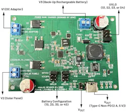
The board pulls in power from two inputs, V1 and V2, which are used to charge the battery and power the load. If the primary power source fails, the solar panel takes over during high sunlight intensity and provides power to the load while charging the battery. At night or when sunlight intensity is weak and the solar-panel voltage drops, the system automatically detects it and switches to battery power to keep the load running.
Assuming a 1S battery configuration, if the battery voltage drops below 3.3 V, the LTC3115-1 will automatically shut down to protect the battery by activating the UVLO feature. This mechanism helps prevent deep discharge, which could damage the battery or reduce its lifespan.
The UVLO threshold can be fine-tuned for each battery configuration by changing resistor values R7, R19, R27, and R21. This will allow the minimum voltage limit to be set as low as 3.0 V depending on the application requirements.
To safeguard the circuit against incorrect battery connections, reverse polarity protection is implemented using a diode (D3) and a fuse (FUSE1). In addition, the input is further protected from reverse voltage scenarios by the body diodes of MOSFETs Q1, Q4, and Q3, which act as a barrier against unintended current flow.
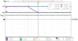
The system’s dynamic behavior under varying load conditions is illustrated through its step response and transient response characteristics in Figure 4, which also shows the performance of the control loop and the effectiveness of the applied compensation network across a range of operating conditions.
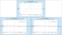
Figure 5 shows the priority switching behavior of the LTC4416 output, as V1 decreases from a higher voltage to 15 V. The device’s output seamlessly transitions to V2 at 8 V, ensuring the output load remains unaffected by the change in voltage. Meanwhile, the V1 restoration point is set to 16.8 V.
Comparison of the Stacked Demo Boards with a Single Board
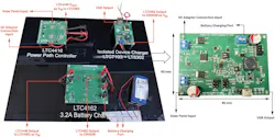
This section presents a detailed comparison between the multi-board prototype and the newly developed single-board solution. In the prototype, the design is comprised of three separate demo boards: the LTC4416 for ideal diode power-path control, the LTC4162-L for battery charging and power management, and the CN0509 USB charger board.
The CN0509 stands out for its wide input voltage range of 5 to 100 V and its ability to provide a regulated 5-V output at up to 2 A. To achieve this, it integrates the LTC7103 buck converter with the LT8302, enforcing galvanic isolation between the input and output stages.
In contrast, the single board consolidates these functionalities by replacing the LTC7103, and LT8302 with a single device: the LTC3115-1. That was done to improve overall system performance by increasing efficiency, reducing physical size, and lowering the cost of the bill of materials (BOM). While the isolated output and other features were sacrificed, the tradeoff is a more practical design that can be scaled up without adding as much complexity.
The implementation of a single-board solution significantly streamlines the overall system design by reducing the BOM count by approximately 30% and its size (Fig. 6). It also cuts out complexity at the system level. By integrating multiple functions on a single board, the design is more space-efficient and scalable, enabling smaller form factors without eroding performance. This is particularly key in applications where space constraints are critical, such as portable electronics.
Fully Integrated Smart Power Bank Saves Power and Space
One of the main improvements is the ability of this single-board solution to run at high efficiency. Optimized power delivery reduces energy losses, which, in turn, supports longer runtimes and better thermal performance.
By minimizing power waste, the single-board solution plays a crucial role in enhancing the system’s performance. As seen in Figure 7, the solution reaches a peak efficiency of 92.94% at an 8-V input and 91% at a 10-V input.
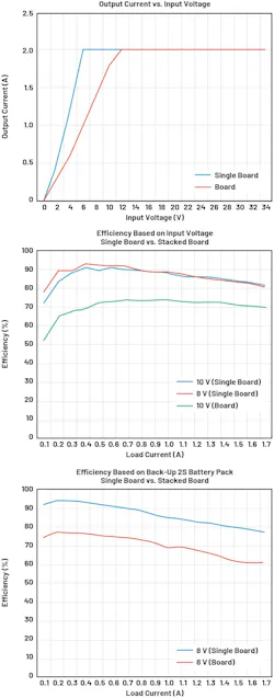
In comparison, the prototype stacked demo board only reached 73.79% peak efficiency at 10-V input. The low efficiency of the stacked solution is clearly due to the energy losses in the cables connecting the boards, as well as the losses in the flyback converter section of the design.
When both input sources fail, the battery automatically powers the load. Using a 2S battery configuration with a nominal voltage of 7.4 V, the single-board solution achieves a peak efficiency of 94.5% versus 77.1% for the prototype stacked demo board. This indicates that the single-board design conserves battery power more effectively during operation, as outlined in Figure 7. The maximum output current of 2 A is achieved from a 6-V input voltage, while the previous prototype achieved a maximum current of 2 A from 12 V.
The single-board architecture of the smart power bank is not only compact and efficient but also flexible, suiting it for a wide range of applications involving battery-powered devices. It supports intelligent power-path management, which will prolong the battery’s lifespan. This concept can be used in embedded automotive systems to combine photovoltaic input with other power-supply sources and battery backup in large-scale production.
Reference
Carey, Diarmuid. “How to Prototype a Power Bank Charger Without Building Any Dedicated Hardware.” Analog Dialogue, February 2023.
>>Download the PDF of this article
dreamstime_dmitriimelnikov_114544075About the Author
Uchechukwu Maduagwu
Applications Engineer, Analog Devices Inc.
Dr. Uchechukwu Maduagwu works as an applications engineer within the Central Applications Team in Dublin. He joined Analog Devices in 2023 and provides design support for the power management portfolio, serving European broad-market customers. Uchechukwu holds postgraduate qualifications from the University of KwaZulu-Natal (UKZN) and University College Dublin (UCD).
Comment About the Article
To join the conversation, and become an exclusive member of Electronic Design, create an account today!
 Leaders Logo
Leaders relevant to this article: