Diving into ESD and EOS Protection in Electronics Design
What you’ll learn:
- How ESD and EOS silently kill electronics and what you can do about it.
- How tiny static sparks bypass factory testing and subsequently cause critical field failures.
- The exact trace geometries and via placements needed to shield sensitive ICs.

In electronics, a single invisible spark can spell the end for costly hardware. This article explains how electrostatic discharge (ESD) and electronic overstress (EOS) can damage sensitive electronics and how to protect designs using practical examples.
Understanding Electrostatic Discharge (ESD)
At its core, electrostatic discharge is the brief flow of electricity that neutralizes different electrical potentials in two objects via contact, an electrical short, or a breakdown in the surrounding air (dielectric breakdown). These charges typically accumulate on a surface through two primary methods:
- Triboelectric charging through physical friction or the separation of two materials.
- Electrostatic induction, which occurs when charges in a nearby object cause charge distribution in another object.
While we often think of static as a minor everyday annoyance, the voltages involved are staggering. A static charge can easily climb into the thousands of volts, which poses a massive threat to modern electronics. As components become increasingly miniaturized and layers become thinner, their tolerance for overvoltage drops significantly. In fact, a spike as low as 10 V is enough to terminally damage some integrated circuits.
The danger of even a single ESD event persists throughout the entire lifecycle of a device, from the design studio and assembly line to daily use by the end consumer. The financial implications are equally significant. A damaged component can cost hundreds of dollars. In high-volume manufacturing, a single ESD issue could compromise an entire production batch.
Therefore, overvoltage protection must be addressed during both manufacturing and development.
Distinguishing ESD from EOS
The terms “electrostatic discharge” and “electrical overstress” are often intertwined, but they differ in their duration and magnitude (Fig. 1):
ESD events are lightning-fast, lasting only nanoseconds. While the peak current is moderate, the voltage is extreme, often reaching into the kilovolts. If you reach to plug a USB cable into your smartphone and a static charge from your clothing jumps to the port, that port intended for 5 V might instantly see 1,500 V.
EOS events last much longer — from milliseconds to several seconds. They typically involve a higher peak current but occur at relatively lower voltages, usually in the range of tens or hundreds of volts. A surge of 400 V in the outlet that hits a connected gadget for several milliseconds is a classic example.
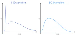
Basically, ESD is a type of EOS event. The latter is caused by various reasons, while ESD is strictly triggered by static electricity.
How Does ESD Damage Electronic Components?
When a high-voltage discharge strikes an unprotected circuit, the resulting damage depends largely on how that energy dissipates through the IC.
ESD causes a massive spike in current. This surge creates an intense, localized heat buildup. In many cases, this thermal energy is sufficient to literally melt the microscopic interconnects, internal wiring, or the delicate semiconductor structures in an IC.
In other scenarios, due to its sheer intensity, the discharge punches through the ultra-thin insulating oxide layers within a component, causing a total system failure or creating hidden vulnerabilities.
The damage from an ESD event generally falls into one of four categories:
1. System malfunction: The PCB or components get no damage, but the discharge disrupts the system’s work, making it freeze or behave erratically. A system reset usually restores full functionality.
2. Data corruption or loss: In these scenarios, the hardware remains physically intact, but the stored information such as user data or even firmware becomes corrupted. A classic example is a nearby lightning strike generating an electromagnetic pulse strong enough to wipe a computer’s hard drive or scramble its memory.
3. Catastrophic failure: This is permanent, irreversible physical damage. It occurs when the electrostatic surge is powerful enough to melt internal metal traces, puncture semiconductor junctions, or destroy insulating oxide layers. The component dies and must be replaced.
4. Hidden degradation: Also known as latent defects, this is perhaps the most insidious type of damage. Here, the internal structure of an integrated circuit gets compromised, but it still works. The problem is that because the device still passes initial testing, these defects are nearly impossible to detect at the factory. Over time, these weakened points degrade further, eventually leading to a critical failure during use. This is a common reason why some brands have a reputation for low reliability. Poor anti-static protocols during manufacturing often lead to a high volume of latent defects.
Industry Standards for ESD and EOS Protection
The IEC 61000-4-2 standard defines four distinct tiers of high-voltage circuit protection to help engineers design hardware that can survive everyday static encounters. Testing involves contact discharge (touching the device with a probe) and air discharge (moving the probe toward the device until a spark jumps). The protection levels are:
- Level 1: Designed for very low-risk environments, withstanding up to 2 kV (contact or air discharge).
- Level 2: A moderate protection level, rated for up to 4 kV (contact or air).
- Level 3: The standard for most industrial and commercial equipment, handling up to 6 kV (contact) and 8 kV (air).
- Level 4: The most robust tier, required for harsh environments, capable of surviving 8 kV (contact) and 15 kV (air).
Strategies for ESD Mitigation
Some techniques can protect hardware from both ESD and EOS, but they’re rarely a complete solution for the latter. Though the two phenomena share similar physical characteristics, their origins require different engineering approaches.
Electrical overstress is generally viewed as abnormal. It should not occur under standard operating conditions. So, EOS immunity is mostly defined by the PCB design. Engineers typically address this by selecting components with a higher absolute maximum rating to make the gadget inherently more resilient. But it still doesn't guarantee survival if those elevated limits are surpassed.
In contrast, ESD events are a near-certainty. There are three distinct ways to protect electronics against them.
1. The ESD-Protected Area (EPA)
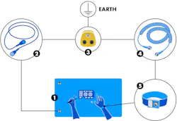
The fundamental goal is to connect every tool, object, and yourself to a common ground, thus eliminating voltage differences. A standard EPA typically includes an antistatic mat, ground cable, grounding plug, ESD loop, and ESD wrist strap (Fig. 2).
For environments requiring higher reliability, engineers employ more sophisticated technology:
- Ionizers flood the air with ions to neutralize static on non-grounded surfaces and remove airborne particles that cause friction-based charging.
- ESD test and measurement equipment to audit the environment. These tools verify that surfaces and personnel remain within safe electrostatic limits.
- Protective packaging such as antistatic bags and ESD-safe boxes. They’re used for storage and transport, preventing charge accumulation during transit.
- Specialized apparel that includes ESD-safe gloves, footwear, and even specialized tape and hand tools designed to bleed off charges safely.
While a strictly managed EPA protects hardware during development, assembly, and testing phases, the device must still be resilient once it leaves the lab. This leads us to the next layer of defense.
2. Integrated Overvoltage Protection on the PCB
Another step is to integrate hardware-level defenses against various electrical threats. These protection components prevent the catastrophic dielectric breakdown of semiconductors and include transient voltage suppressors (TVS diodes), metal-oxide varistors (MOVs), and gas discharge tubes (GDTs).
- TVS diodes offer sub-nanosecond response times and low capacitance. They’re the gold standard for ESD protection in PCB design.
- MOVs are passive components that can absorb much larger energy surges than diodes, though they’re slower and degrade over time. MOVs are typically deployed in AC power supplies and industrial equipment to clamp transient voltage spikes.
- GDTs are gas-filled spark gaps that handle the heaviest electrical loads by creating a virtual short circuit. But their slow response time (tens of nanoseconds) means they’re usually placed at the very front of telecommunication lines or main AC inputs, often paired with a faster TVS diode downstream to catch the initial voltage peak.
The scheme below shows how a TVS diode works (Fig. 3).
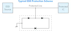
The TVS array is connected in parallel with the protected IC. Under normal voltages, the TVS maintains extremely high resistance. But when the voltage rises beyond the diode’s avalanche breakdown threshold, its resistance drops instantly, making the current flow safely to ground. Once the voltage returns to normal, the TVS resets to its high-resistance state.
Engineers must place such components at every “entry point” where static electricity could penetrate the system. This usually includes external connectors (USB ports, Ethernet jacks, and power inputs) and user interface elements (mechanical buttons, switches, and keyboard matrices).
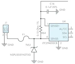
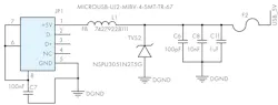
For instance, at Integra Sources, we developed a medical-grade electrocardiogram (ECG) system where it was critical to safeguard several external interfaces. One particular entry point was the battery connector (J1). We put the NSPU3051N2T5G (TVS1) in parallel immediately following the connector (Fig. 4).
Another external interface was USB. Here we made a custom solution instead of using specialized TVS arrays (Fig. 5). The capacitors are intended to filter low-frequency EMI and don’t provide ESD suppression.
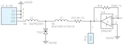
Another entry point was the electrodes designed for direct skin contact (Fig. 6). Note: The op amp (U6) here can function as another protection component because the output pin (1) has very low resistance. The resistor (R15) was put here for protection from residual pulses.
3. Strategic PCB Design to Suppress ESD
While a protective component acts as the “gate,” the PCB layout must provide the “highway” for excessive energy to escape safely to the ground.
Managing impedances
Every trace and component in a PCB has a small amount of parasitic inductance. A typical protection circuit contains four (Fig. 7).
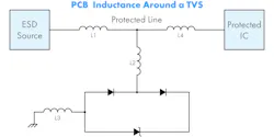
The goal is to make L4 significantly larger than other inductances. By increasing the impedance of the path leading to the IC, we force the energy to take the “easier” path to the ground.
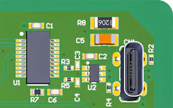
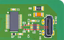
Practical example: Take, for example, this PCB from another project developed by Integra Sources. To shield the UART chip (U1) from static entering through USB, we used a USBLC6-4SC6 ESD suppressor (U2).
There are two critical design choices that significantly enhance the component’s effectiveness:
- We positioned U2 as close to USB as possible. This minimizes L1 and maximizes L4, effectively steering any incoming discharge into the suppressor before it can travel further.
- We put U2 directly on the path between the connector and the IC to effectively eliminate L2.
Mitigating electromagnetic interference (EMI) from ESD events
Being a high-speed transient, an electrostatic discharge generates a powerful, rapidly shifting electromagnetic field. It can capacitively or inductively couple onto adjacent traces, inducing “ghost” voltages in circuits that weren't even part of the original discharge path.
To contain this interference, our design strategy focuses on two key areas:
- First, the section between the USB and the TVS generates EMI. We strictly avoid placing any sensitive or unprotected circuitry in the immediate vicinity of these traces.
- Second, high-frequency transients like ESD are particularly sensitive to the physical shape of a trace. Sharp, 90-degree corners can radiate significant EMI. To minimize this, engineers must use short and direct paths, or 45-degree corners if that’s not an option.
Optimizing via placement for ESD suppression
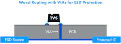
If a via is placed incorrectly, its parasitic inductance can create a “fork in the road” for an ESD pulse, inadvertently directing some energy toward a sensitive IC rather than the protection device.
In Figure 10, the via acts as L2. Despite the TVS, the current will branch, with a significant — and potentially destructive — percentage flowing straight into the IC. This layout should be avoided at all costs.
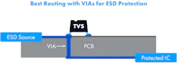
The best option is to keep the source and the TVS on the same physical layer (Fig. 11). This ensures the transient current must literally pass the TVS before it ever encounters a via. By making the TVS the first stop on the signal path, we ensure the bulk of the energy is shunted to ground immediately.
In dense designs, such as the USB interface mentioned above, placing everything on a single layer isn't always feasible. But there are alternative acceptable configurations.
Even when layers must be swapped, it’s the same principle: force the current through the TVS first. In the project, two ESD sources and the protected IC were on three different layers. So, we placed the TVS diode on the same layer as the IC (Fig. 12).
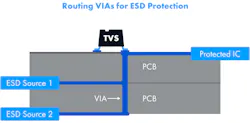
If you can’t implement this layout, one particular option is to direct the current to another layer with the TVS and then back (Fig. 13).
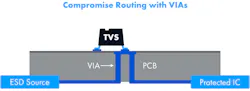
This method isn’t perfect but can work if the engineer has no other options.
Conclusion
Electrostatic discharge and electrical overstress aren’t minor nuisances — they’re critical threats to hardware longevity and brand reputation. Protecting electronics from these silent killers requires a multi-layered strategy that goes far beyond simply adding a few components to a schematic. It’s a holistic process that includes environmental control, component selection, and PCB layout.
Whether you’re designing a consumer gadget or a life-critical medical device, prioritizing ESD and EOS immunity from the very first day of development is the only way to prevent costly field failures and latent defects.
>>Download the PDF of this article
 promo
promoAbout the Author
 Andrey Solovev
Andrey Solovev
Chief Technology Officer, Integra Sources
Andrey Solovev, CTO of Integra Sources, has 20 years of experience in the IT field. He possesses unique skills, as he has tremendous hands-on experience in electronics design and software development backed by fundamental knowledge of mathematics, physics, engineering, and programming.
Andrey has a Ph.D. in physics and mathematics. He has written over 20 scientific papers on automated spectral analysis, analog-digital converters, electro-optical diagnostics systems, and other topics. For 16 years, he has been a practicing university teacher. Andrey successfully combines technical management in the company with conducting university classes on system programming and robotics programming.
Under Andrey's technical guidance, Integra Sources has become one of the world's best development companies in various IT categories, according to prestigious research organizations.
Andrey often participates in IT meetings, exhibitions, seminars, and conferences, where he can share his rich experience in custom electronics design and software development and adopt the world's greatest achievements in this area.
Andrey takes an active part in editing and saturating the blog's articles with high-quality technical information.
Comment About the Article
To join the conversation, and become an exclusive member of Electronic Design, create an account today!
 Leaders Logo
Leaders relevant to this article: