Powering the Isolated Side Of A Half-bridge Configuration
The half-bridge topology is widely used in power converters and motor drives. This is largely due to the half-bridge’s ability to provide efficient synchronous control of a pulse width modulated (PWM) signal over the bus voltage, however, between the controller and the power devices, gate drivers are often required to obtain faster switching times, and provide isolation for either safety and/or functional purposes. For systems with bus voltages that are above the maximum power switch gate-to-source voltage limits, the gate drives must be supplied with voltages other than the system bus.
Related Articles
- High Current Development Board Featuring Multiple Half-Bridges in Parallel
- 85-V Half Bridge MOSFET Driver Has Adaptive Dead Time, Shoot-Through Protection
- Expanded µIPM Family Has Half-Bridge Power Modules
- Applying Synchronous Rectification in Resonant Half-Bridge Converters
- Synchronous MOSFET half bridge offers 90% efficiency
Here, various gate drive powering options, basic design constraints, and trade-offs are presented to help the designer choose which topology to use. These include the isolated gate drive transformers, as well as powering optocouplers or digital isolators with isolated DC-DC fed gate drivers, bootstrap configurations, and isolated gate drivers with internal DC-DC voltage sources.
For higher power systems, the power switching devices are a large part of the BOM cost, and N-type devices typically have lower on resistance than P-type devices of the same size and cost [1]. Additionally, by using two identical switches in a single leg of a half-bridge setup, designing around timing requirements such as non-overlap and dead-time can be simplified. For these reasons, half-bridge configurations typically consist of two N-type devices, whether they are NPN BJTs, NMOS devices, or N-type IGBTs. For simplicity, we will refer here to half-bridge configurations that use two NMOS devices per leg, but the same principles can be applied to IGBTs as well. In order to use BJT devices, constant base current should be accounted for in the design.
Basic Gate Drive Requirements
Consider a typical half-bridge configuration as shown in Fig. 1. The MOSFETs are operated in a mutually exclusive fashion, because if both were conducting at once, shoot-through would occur. For a MOSFET to turn on, VGS > VT where VGS is the gate to source voltage and VT is the threshold voltage of the particular MOSFET. It is recommended to have sufficient overdrive of MOSFETs in operation, so actual gate voltages are VGS >> VT in most applications. For the part of the switching period where, the low-side switch, Q2, is on, and the high-side switch, Q1, is off. This means that VG1S1 < VT, and VG2S2 >> VT. For many systems, a VG1S1 of 0 V is sufficient to keep the high side switch off. In the ideal case, VOUT swings close to the system ground.
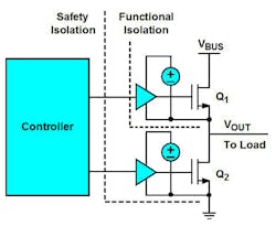
Ignoring dead-time requirements, the other part of the switching cycle has Q1 on and Q2 off, meaning VG2S2 < VT, and VG1S1 >> VT. During this time, VOUT swings close to the bus voltage. Note that the source of the high-side switch is connected to VOUT, which means the gate of Q1 goes above the bus voltage for part of the switching cycle.
If the controller IC were connected directly to the gate of Q1, a voltage greater than VBUS + VT would be required of the IC, which is not feasible in many cases.
One of the main purposes of a gate driver is to provide fast switching times to the power switches, allowing for faster rise and fall times. This reduces losses in the power stage associated with slew rates. Drive strength has been measured in peak current in the past, or more precisely in driver RDSON. It is useful to note that the power requirements for a gate driver with higher peak current (or lower RDSON) are not necessarily higher, as the power required to switch a gate is mostly driven by:
Q×V×FSW
Where:
Q = Gate charge
V = Gate voltage swing
FSW = Switching frequency of the system [2]
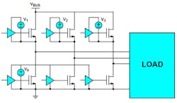
In order to power the gate driver on the high-side switch, the power source must be able to follow the VOUT voltage, since the gate is referenced to this voltage. Adequate decoupling can often resolve any voltage spikes seen due to the fast changing of the isolated power supply’s ground reference. Additionally, each gate driver that does not share a common ground can require its own isolated power supply. Consider a typical three-phase system, consisting of three half-bridge legs as shown in Fig. 2. There are a total of four separate ground references in the system, since the low-side switches share a common reference. Depending on whether safety or functional isolation is required, a three-phase system requires either three or four dedicated power supplies.
Two requirements that factor into any project are solution size and total solution cost. There are tradeoffs that will be explored in the different options. The basic requirements for delivering isolated power to a gate driver can be summarized as:
1) Deliver sufficient voltage swing
2) Voltages above the bus value for part of the switching cycle
3) Floating ground that can follow the half-bridge midpoint voltage
4) Sufficient drive strength
5) Compact solution size
6) Reasonable cost
Gate Drive Transformers
One of the earliest solutions to delivering an isolated gate signal was using gate drive transformers like the system pictured in Fig. 3. In this system, energy is transferred across a transformer, creating the necessary gate voltages on the secondary side. One benefit of this system is that guaranteed complimentary operation is relatively easy to achieve by having one of the secondary outputs of opposite polarity to the other. In this manner, to drive the high-side gate on, and the low-side gate off, current is fed into the transformer primary in one direction, and driving current in the opposite direction drives the gates to their opposite states.
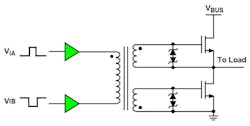
Since gate drive transformers act as the power source for the gate drive, there is solution size savings near the gate being driven. The parts count is also lower as a dedicated isolated power supply is not needed. The actual cost of the transformers varies between moderate to expensive.
Transformers can’t pass DC current, so in the most basic topology, the gate sees a zero volt-second balance, meaning as duty cycle increases, the peak positive voltage decreases [3]. This puts limitations on the operating duty-cycle, and makes tuning dead-times challenging. Fast changes in duty cycle can also lead to core saturation balancing issues. There are DC-restored topologies, but care must be taken on shutdown, or shoot-through can easily occur, making gate drive transformers less suitable for applications requiring fast shutdowns, such as when a system fault is detected.
The core of the gate drive transformer must be reset, or risk saturation, putting further design constraints on the switch timing. For the above reasons, gate drive transformers have largely fallen out of favor for higher reliability, high performance systems.
Dedicated Isolated Supplies
Another method of isolating the gate drive is to transfer the timing information using isolators. Optocouplers use light to transmit the timing data across an isolation barrier to a phototransistor or photo-diode. The internal diodes light output drops with age and/or temperature, leading to a timing shift that necessitates wider margins on dead-times [4]. As an alternative to optocouplers, digital isolators typically transfer the timing information through inductive or capacitive coupling, resulting in effectively no timing shift due to aging, and dramatically less shift due to temperature than optocouplers. In both optocouplers and digital isolators, an output buffer of the transmitted signal delivers the final drive strength to the gate. This buffer can exist inside or outside the isolator package. High-voltage level shifters transmit timing data to the high side through use of pull-up structures that can take hundreds of volts. High-voltage level shifters can be susceptible to latch-up if the half-bridge voltage rings negative, an issue not found in digital and optocoupler isolators.
The most straightforward method of powering the buffer is to provide a dedicated isolated DC-DC converter for each floating region of the half-bridge. For a multi-leg system, the low-side gate drivers can share a voltage source as long as the current output is sufficient, as seen in the example system in Fig. 2.
Dedicated isolated power supply setups have no duty-cycle or minimum switching frequency requirements, and the inputs of the isolated gate driver can be independently controlled, allowing for dead-time tuning. This comes at the cost of a larger solution size and cost due to the extra components. An isolated power supply can be created at a system level by topologies such as the flyback or forward converters that include transformers. There are also monolithic modules such as those available from Recom that are designed specifically to allow for high isolation voltages [5].
Half-bridge Bootstrap Configuration
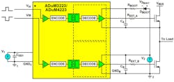
Outside of quiescent currents, the output side of an isolated gate driver mainly takes current from the supply rail when driving the gate towards high. Once the gate voltage of an IGBT or MOSFET reaches the supply rail, the dissipation is minimal as the gate is essentially a capacitor. For the high-side driver, this current draw coincides with the time the half-bridge voltage is being pulled to the bus voltage as the high-side MOSFET turns on. This also means that just before the highest current draw, the high-side ground is tied to the low-side ground by the low-side power switch. By using a single diode, and a suitably large capacitor on the supply rail of the high-side, a temporary voltage source can be provided as shown with an ADuM3223 in Fig. 4. A resistor is shown in series with the bootstrap diode in order to control peak charging current. [6]
The bootstrap capacitor is charged during the on-time of the low-side switch, and discharges quickly to fill up the gate capacitance but slowly discharges during the on-time of the high-side switch due to the high-side driver’s quiescent currents. This leads to constraints on the system duty-cycle and switching frequency [7]. As long as there is sufficient time to charge the bootstrap capacitor, and the high-side switch is not on for longer than the capacitor can support, this solution excels in cost and solution size metrics, especially in multi-phase systems. Additionally, multiple bootstrap capacitors can be charged at once by turning the low-side switches on at the same time during startup.
Integrated Power and Gate Driver
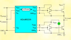
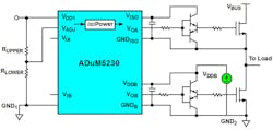
The natural progression towards smaller solution size is to create a single IC with isolated power and gate driver capabilities. The most efficient way to transfer isolated power is through inductive coupling. Optocouplers and capacitive couplers would require too large an area, be too slow, and have too much energy loss to support such as system. For circuits that use an all-inclusive isolated power and gate driver topology, small chip-scale inductors can be employed within the IC. One such system, using the ADuM5230, is shown in Fig. 5. This solution contains transformer coils to transmit timing information as well as coils to transfer power to the high-side driver, eliminating the need for an extra external isolated power supply on the high-side [8]. External buffers increase the peak current output, allowing for the driving of larger gate capacitances. Due to efficiency limits, the maximum power dissipation, and therefore switching frequency and/or max gate charge load is limited. As the technology progresses, monolithic solutions for higher system requirements will begin to emerge.
Outside of power constraints, the integrated isolated power and gate driver systems provide excellent solution size, as well as remove duty-cycle and switching frequency minimums.
Conclusion
Powering the isolated side of your half-bridge configuration presents some unique challenges, but many topologies exist for the designer. Gate drive transformers excel in part count, but are limited by complexity of drive signal, and limitations due to the magnetic core dynamics. Dedicated isolated supplies can remove duty-cycle and frequency requirements, with the drawback of cost and solution size. If duty-cycle and switching frequency can be constrained, the half-bridge bootstrap configuration is inexpensive and can greatly reduce part count and solution cost. Some highly integrated solutions exist, with the power transfer occurring with internal transformers, saving solution size, and parts count. With the many topologies shown, a designer has the tools to create a robust half-bridge solution
Powering the isolated side of your half-bridge configuration presents some unique challenges, but many topologies exist for the designer. Gate drive transformers excel in part count, but are limited by complexity of drive signal, and limitations due to the magnetic core dynamics. Dedicated isolated supplies can remove duty-cycle and frequency requirements, with the drawback of cost and solution size. If duty-cycle and switching frequency can be constrained, the half-bridge bootstrap configuration isinexpensive and can greatly reduce part count and solution cost. Some highly integrated solutions exist, with the power transfer occurring with internal transformers, saving solution size, and parts count. With the many topologies shown, a designer has the tools to create a robust half-bridge solution.
References
[1] C. Hu, “Modern Semiconductor Devices for Integrated Circuits”. Prentice Hall; 2009
[2] Concept, “IGBT and MOSFET Drivers Correctly Calculated”, Appl. Note An-1001, pp. 1.
[3] R. Ridley, “Gate Drive Design Tips,” Power Systems Design Europe, 2006, pp. 14-18.
[4] R. Ripas, “Gauging LED Lifetime in Optocouplers”, Machine Design, Sep 20, 2012.
[5] Recom, “ECONOLINE DC/DC-Converter,” RP Series datasheet, Rev. 0, 2014.
[6] Analog Devices, Inc., “ADuM3223”, Datasheet, Rev. D, http://www.analog.com/en/interface-isolation/digital-isolators/adum3223/products/product.html, 2014.
[7] J. Adams, “Bootstrap Component Selection for Control IC’s”, International Rectifier, Design Tip DT 98-2.
[8] Analog Devices, Inc., “ADuM5230”, Datasheet, Rev. B, http://www.analog.com/en/interface-isolation/digital-isolators/adum5230/products/product.html, 2013.
About the Author
Ryan Schnell
Applications Engineer, Analog Devices
Ryan Schnell is an Applications Engineer at Analog Devices. Ryan has a background in power and control systems. His current focus is on defining and developing isolated gate drivers that use iCoupler technology. He holds a BS and an MS in electrical engineering, and a PhD in power electronics from the University of Colorado.
Comment About the Article
To join the conversation, and become an exclusive member of Electronic Design, create an account today!

Leaders relevant to this article: