Inside-the-Package Isolation for SiC MOSFETs

As power electronics pile in and around the electric grid, silicon carbide (SiC) sits inside a lot of it. SiC is breaking into renewable-energy systems such as grid-tied solar and wind inverters and battery energy storage systems (BESS) due to its unique material properties, offering low on-resistance, high thermal conductivity, high breakdown voltage, and fast switching speeds compared to silicon. Given all that, it’s also being integrated into solid-state transformers (SSTs) intended for AI data centers and DC fast chargers.
But in the drive for higher power density, SiC MOSFETs are piling into increasingly hot and overcrowded systems while handling higher operating voltages.
For instance, Navitas Semiconductor and École Polytechnique Fédérale de Lausanne (EPFL) University co-developed a modular SST platform based on a single-stage bridge-rectifier architecture. Each cell converts 3.3 kV AC to 800 V DC at 250 kW and puts everything into a form factor as small as a briefcase. Several building blocks can then be linked, creating larger SST systems capable of handling high grid-level voltages up to 34.5 kV.
SiC is uniquely suited to these situations, using its higher breakdown voltage to run at high voltages with lower conduction losses than silicon, its wider bandgap to operate at higher junction temperatures, and its higher saturation velocity and electron mobility to enable higher switching frequencies. These properties all enable more compact, efficient power converters. But pushing the power limits of SSTs and the like without compromising safety or reliability creates new challenges. Higher power densities concentrate heat, while higher operating voltages increase insulation and isolation requirements.
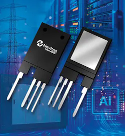
Now, Navitas is trying to tackle these dual challenges with its new isolated TO-247-4 package: the UHV‑TO‑247‑4‑ISO. Featuring 12 mm of pin-to-pin creepage distance and more than 6,000 V of integrated high-voltage isolation, the package is purpose-built for 1,200- to 3,300-V SiC MOSFETs. Navitas said it delivers “module‑like” performance while offering the flexibility and compact form factor of a discrete device package (Fig. 1).
Bringing Ceramic Substrates Out of the Module and Into the Package
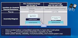
The isolated TO‑247‑4 integrates the same aluminum-nitride (AlN) substrate widely used in SiC power modules to provide high-voltage isolation — within the package itself. By integrating the isolation barrier, it eliminates the need for external isolation components to establish safe, reliable operation between high- and low-voltage circuits. The through-hole package is also designed for integration into liquid-cooled systems to manage the thermal demands of densely packed power converters.
The ceramic substrate in the package is based on active metal brazing (AMB) technology for high-voltage isolation. It comes with a robust reflow-compatible heatsink interface for heat removal, simplifying the system stack. That also enables superior power cycling capability and thermal cycling lifetime.
As with the widely used TO‑247‑4, the package includes a dedicated signal source terminal (Kelvin connection) for the gate drive, which reduces parasitic inductance and switching losses.
One of its other advantages is that it can be directly cooled. The thermal pad inside the package means that it can mount directly to liquid- or air-cooled heatsinks, eliminating the need for thick thermal paste (TIM) between them (Fig. 2). This reduces the thermal resistance between the die and the heatsink (RTH,J-HS) by up to 60%, giving it the ability to remove significantly more heat from the SiC MOSFET. What that means is space and cost savings at the system level as well as higher reliability, said Navitas.
When compared with non-isolated packages in the same class, Navitas noted that it can also reduce coupling capacitance and EMI. The in-package, high-voltage isolation reduces stray capacitance between the die and heatsink compared to external isolators, effectively minimizing common-mode noise (CMTI) and radiated EMI. This allows for higher switching speeds, which translates to higher power density and efficiency at the system level. It also reduces system-level costs associated with EMI mitigation.
Isolated SiC for Grid-Connected Power Electronics
Said Paul Wheeler, VP and GM of the SiC business unit at Navitas, “High-power system design is fundamentally challenged by the need to balance efficient thermal management with robust high-voltage isolation.”
Wheeler added that the easy-to-cool, high-voltage package “overcomes critical thermal and isolation challenges, delivering power module-class performance in a compact discrete form factor” that can fit into next-generation applications like immersion-cooled and liquid-cooled power electronics.
According to Navitas, the breakthrough is a boon for high-voltage, grid-connected power-conversion systems (PCS), SSTs, BESS, and renewable-energy infrastructure, which are all rapidly adopting SiC. A large-scale, grid-tied BESS often uses DC bus voltages of up to 1,500 V DC to leverage the advantages of high-voltage operation, and the solar inverters and other renewable-energy systems often feeding into them are also shifting from 1,000 V to 1,500 V.
One of the most promising technologies for modernizing the data center so that it can keep up with the needs of AI is the SST. In data centers, STTs are being developed to step down the utility-level AC power at 13.2 or 34.5 kV directly to the OCP-backed ±400 V or NVIDIA-backed +800 V DC outputs that connect to AI server racks. These systems can eliminate bulky iron and copper line-frequency transformers (LFTs) that currently act as front-end power distributors in AI data centers.
SSTs are usually based on multi-level converters that distribute the grid-level voltages between lots of cells, each equipped with high-voltage switches. In the SST co-developed with EPFL, Navitas used its 3,300- and 1,200-V SiC trench-assisted planar (TAP) MOSFETs.
Navitas said the UHV-TO-247-4-ISO is offered in SiC MOSFETs with 3,300-, 2,300-, and 1,200-V ratings. The new package, together with its direct cooled heatsink assembly, was on display at PCIM 2026.
About the Author

James Morra
Senior Editor
James Morra is the senior editor for Electronic Design, covering the semiconductor industry and new technology trends, with a focus on power electronics and power management. He also reports on the business behind electrical engineering, including the electronics supply chain. He joined Electronic Design in 2015 and is based in Chicago, Illinois.