Shielded Power Inductors Target Space-Constrained Portable Electronics
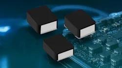
The SRP201210V Series Shielded Power Inductors is a new family of compact power inductors designed for applications where board space, profile height, and power capability must be carefully balanced. Developed by Bourns, the series combines a metal-alloy powder core with magnetically shielded construction to support high current handling while limiting magnetic field radiation in dense electronic assemblies.
The low-profile design, featuring a maximum height of 1.0 mm, helps engineers address space constraints in applications such as wearable devices, smartphones and tablets, SSDs, IoT modules, and other products where size, efficiency, and low EMI are critical.
In addition to their shielded construction, the inductors are equipped with low DC resistance characteristics. They allow designers of portable electronics to incorporate more functionality within smaller form factors while minimizing EMI-related design concerns and maintaining thermal performance.
The series offers inductance values from 0.24 to 0.47 µH and operates across a temperature range of −55 to +125°C. Full specifications, ordering information, inventory status, and sample requests are available through its product page.
About the Author
 Lee Goldberg
Contributing Editor
Lee is the author of the popular PowerBites series.
Lee Goldberg is a self-identified “Recovering Engineer,” Maker/Hacker, Green-Tech Maven, Aviator, Gadfly, and Geek Dad. He spent the first 18 years of his career helping design microprocessors, embedded systems, renewable energy applications, and the occasional interplanetary spacecraft. After trading his ‘scope and soldering iron for a keyboard and a second career as a tech journalist, he’s spent the next two decades at several print and online engineering publications.
Lee’s current focus is power electronics, especially the technologies involved with energy efficiency, energy management, and renewable energy. This dovetails with his coverage of sustainable technologies and various environmental and social issues within the engineering community that he began in 1996. Lee also covers 3D printers, open-source hardware, and other Maker/Hacker technologies.
Lee holds a BSEE in Electrical Engineering from Thomas Edison College, and participated in a colloquium on technology, society, and the environment at Goddard College’s Institute for Social Ecology. His book, “Green Electronics/Green Bottom Line - A Commonsense Guide To Environmentally Responsible Engineering and Management,” was published by Newnes Press.
Lee, his wife Catherine, and his daughter Anwyn currently reside in the outskirts of Princeton N.J., where they masquerade as a typical suburban family.