This Week in PowerBites: Solar-Panel Breakthrough and Lots of BMS
This article is part of the Power Management Series: This Week in PowerBites
Film-Based Perovskite PV Module Achieves Record 15.1% Conversion Efficiency
Toshiba Corp. recently announced a new coating method for the perovskite-based thin-film solar panels that boosts the efficiency of its 703-cm2 polymer film-based perovskite photovoltaic module1,2 to 15.1%—the highest for any large-area panel of its type. The innovative coating method for the perovskite layer also greatly reduces production time and costs, helping reduce overall cost for solar-power generation.
The panels’ increased efficiency, combined with their lighter weight, has the potential to make them an attractive alternative to conventional crystalline panels. The weight and rigidity of crystalline panels makes it difficult to use them in locations such as low load-bearing roofs and office windows.
The new perovskite-layer coating method is an improvement on the two-step coating process originally used to produce the company’s thin-film solar panels. In that process, the first layer of PbI2 (lead iodide) ink was applied to a substrate, followed by a layer of MAI (methyammonium iodide, CH3NH3I) ink, triggering a reaction that formed an MAPbI3 layer. While commercially successful, this process had a low coating rate and often left unreacted sections in the perovskite layer (Fig. 1, left). An earlier one-step process was developed that applies MAPbI3 ink directly. Though promising, it was difficult to control the crystallization of the MAPbI3 enough to maintain a uniform thickness of the perovskite layer across a large area (Fig. 1, right).
The one-step meniscus coating method is over 25X faster than the previous two-step process (left). The current-voltage curve (IV curve) shows PCE raised to 15.1% for the 703-cm2 polymer film-based module.
Toshiba estimates that if all roofs in Tokyo5 (approx. 164.9 km2) were covered with the new PV modules, they would generate power equivalent to two-thirds of the annual power consumption of the city's homes.4 The company says that its goal is to increase the efficiency of their perovskite PV modules to 20% or more, and to enlarge the active area to 900 cm2, the size required for practical application. In doing so, the company estimates that the improvements will reduce their manufacturing cost to roughly $0.14/W.
The new coating technology and the perovskite solar modules it made possible are the result of research done under a New Energy and Industrial Technology Development Organization (NEDO) project: Development of Technologies to Promote Photovoltaic Power Generation as a Main Power Source. You can read the full article here.
References
1. The active area is 24.15 × 29.10 cm (702.765 cm2).
2. Toshiba survey of 100 cm2 or larger film-based perovskite solar modules with a plastic substrate (9/10/2021).
3. Toshiba’s survey.
4. 2018 annual power consumption by homes in Tokyo: 26 × 109 kWh. Source: Agency for Natural Resources and Energy, Ministry of Economy, Trade and Industry.
5. Toshiba estimate. Total roof area (164.9km2) in Tokyo. J. Archit. Plann, AIJ, No. 581, 83−88, July 2004.
BMIC Boosts Fuel-Gauge Accuracy and Battery Runtime While Shrinking Solution Size
The MAX17330 battery-management IC (BMIC) for one-cell lithium-ion/polymer batteries, developed by Analog Devices, features an integrated fuel gauge and advanced battery protection that delivers longer battery runtime for consumer applications and similar products. ADI’s proprietary AccuCharge and ModelGauge technologies, which deliver high top-off charge and deep safe discharge, enable longer run-time of medical and fitness wearables, home and building automation sensors, handheld computers, and terminals. The MAX17330 also simplifies battery management for devices using parallel cells, such as foldable smartphones and tablets, as well as AR/VR smartglasses.
The MAX17330 improves on the techniques used by conventional battery-charger ICs, which can result in inconsistent charging unless they have additional margin for the battery protector, preventing the battery from being charged to its maximum level. The MAX17330 also addresses the challenges of multi-cell designs where the cells are physically separated by controlling the charger using its integrated fuel gauge for each individual cell.
Features include:
- 20% more accurate charging with AccuCharge technology delivers higher top-off charge for longer runtime.
- The ModelGauge m5 fuel-gauge algorithm delivers 40% more accurate state-of-charge (SOC) readings; EZ configuration eliminates any need for battery characterization.
- A small wafer-level package (WLP) and integration of the battery charger, fuel gauge, protector, and authenticator functions reduce the total solution size by 36% when compared to similar solutions.
For more information, check out the MAX17330 battery-management IC product page, download the datasheet, and order samples here. And to learn more about ADI’s AccuCharge and ModelGauge technologies, go here.
Battery-Management System for Low-Voltage EVs Enables Hot Swapping to Cut Charging Time
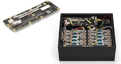
Sensata Technologies' i-BMS is a cell chemistry-agnostic, compact, integrated battery-management system (BMS) developed for the cost-optimized mass production of applications up to 60 V, such as 2- and 3-wheelers, automated guided vehicles (AGVs), and robotics. The new system, developed by the company’s Lithium Balance product brand, acquired by Sensata earlier in the year, provides hot-swap functionality and parallel battery-pack support that make it possible to quickly exchange depleted batteries with fully charged batteries.
i-BMS's parallel pack support allows for the use of two or more battery packs in parallel. As a result, OEMs of 2- and 3-wheelers can implement smaller battery modules, improving the safety and serviceability of the battery system. For example, if one battery cell fails while in use, the issue is isolated to that one faulty module, which is easier to replace than the entire system. Meanwhile, additional battery packs can continue to provide power.
Though measuring only 65 × 200 mm (2.6 × 7.9 in), the i-BMS PCB board is equipped with everything required to manage and maintain a battery system without the need for any external components, making it a convenient and cost-efficient design for mass production. All critical components are pre-integrated into the system, including a pre-charge circuit, on-board current measurement, MOSFET power switches for battery disconnect, and a dc-dc power supply. The solution features key components that are ASIL C safety rated and include self-test capabilities for safety-critical measurement circuits.
Advanced Software Helps Maximize Battery Use
Sensata’s BMS software incorporates advanced algorithms that ensure accurate state-of-power (SOP) predictions based on cell internal resistance, voltage, and current constraints, precise state-of-charge (SOC) calculations, and state-of-health (SOH) calculations based on aging effect. The high degree of accuracy in assessing the state of the battery allows for a more precise battery system, helping customers maximize battery utilization as well as increase range, uptime, and performance of the vehicle.
In addition, the BMS Creator configuration software allows the battery-pack designer to create a unique battery setup by defining application-specific BMS parameters and safety strategies, optimizing battery operation. Other advanced software features include the ability to measure rate of change of temperature to predict thermal runaway, dynamic regulation of current in extreme thermal conditions, as well as advanced parameter settings for CAN communication.
To learn more about the new i-BMS, visit www2.sensata.com/ibms.
100-V MOSFET Process Dramatically Improves Performance, Reliability for High-Switching-Frequency Apps
According to Infineon Technologies, its latest power MOSFET technology addresses the growing need for higher efficiency and improved reliability in modern switch-mode power supplies (SMPS) and battery-powered applications. Its new OptiMOS 6 100-V technology is optimized for high-switching-frequency applications such as telecom and solar, where losses are associated with charges (switching) and on-state resistance (conduction). In addition, the devices' very low RDS(on), excellent figures-of-merit (FOMs), and wider safe operating area (SOA) suit them for battery-powered applications (BPA) and battery-management systems (BMS).
The unique features of OptiMOS 6 allow for easier thermal design and less paralleling, leading to improved efficiency and power density, reduced system cost, and prolonged lifetime.
OptiMOS 6 provides unique advantages for the telecom market by achieving 18% lower RDS(on) and more than 30% improvement in FOMs (RDS(on) x Qg and Qgd) compared to the previous OptiMOS 5 process. In a 600-W, −(36-60)-V to 12-V ZVS buck-boost converter, the OptiMOS 6 in SuperSO8 package with 2.2 mΩ can achieve 1% higher efficiency than the OptiMOS 5 BSC027N10NS5 (2.7 mΩ) across the whole load range. This results in a 7-W lower power loss due to improved charges and RDS(on), enabling up to 15% higher power density. Other key benefits are lower conduction and switching losses and minimization of paralleling parts.
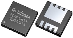
The OptiMOS 6 100 V is available in SuperSO8 5×6 and PQFN 3.3×3.3 packages in a broad range of RDS(on) classes from industry best-in-class to price/performance optimized. More information is available at www.infineon.com/optimos-6-100V. And for more about the company’s contribution to energy efficiency, check out www.infineon.com/green-energy.
Port-Protection IC for STM32 MCUs Tailored to USB-C Dual-Role Power
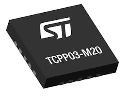
STMicroelectronics' TCPP03-M20 USB Type-C port-protection IC is intended for dual-role power (DRP) applications, enabling designers to simplify the design of products that can act as a power source for connected devices as well as accepting power from other USB-C sources.
When used as a companion chip with STM32G0*, STM32G4, STM32L5, and STM32U5 microcontrollers that contain ST’s UCPD (USB Type-C and Power Delivery) interface IP, the TCPP03-M20 enables a cost-effective partitioning of the USB Type-C implementation. Product designers can achieve a two-chip solution with the STM32 as the host microcontroller, saving bill-of-materials costs, PCB space, and circuit complexity.
As defined in the USB Type-C specification, a USB-C dual-role device, such as a smart speaker, smartphone, tablet, laptop, or camera, must have the ability to dynamically change their power role from sink to source as well as their USB data role from device to host (and vice versa). This enables new use cases to preserve and share energy between battery-powered devices, as well as extend device interoperability. The USB DRP capability defined in the Type-C specification allows any USB devices with the ST chip inside to charge the battery of a connected device.
The TCPP03-M20 is fabricated using the company’s bipolar, CMOS, and DMOS (BCD) process that can combine logic and high-voltage circuitry on the same chip, enhancing integration and reliability. The technology also enables ±8-kV ESD protection (IEC61000-4-2 Level 4), overvoltage, and overcurrent protection to be implemented on the same chip. These are needed to guard against unintended short-circuits or connection of defective equipment, as well as comply with the USB-C Power Delivery specification.
The chip integrates switches for the USB-C port VCONN and CC lines, a charge pump with two N-channel MOSFET gate drivers for source and sink power path, VBUS and VCONN power-path discharge circuitry, and dead-battery management.
Standalone power sink and source applications are handled using ST’s TCPP01-M12 and TCPP02-M18 BCD ICs, respectively. Like all ST’s TCPP products, the TCPP03-M20 is compliant with the latest features of the USB-C PD specification 3.1 Standard Power Range (SPR), including PPS (programmable power supply).
Projects using the TCPP03-M20 for DRP applications up to 10 0W can be developed using the STM32 Nucleo expansion board, X-NUCLEO-DRP1M1, and X-CUBE-TCPP STM32Cube expansion software, which includes application code examples. Developers also can take advantage of support for UCPD configuration in STM32CubeMX, the STM32G071B-DISCO USB-C sniffer, and the STM32CubeMonitor-UCPD debug tool. The X-NUCLEO-SNK1M1 board is available for sink applications, and the X-NUCLEO-SRC1M1 for Power Delivery Source development is planned for release in Q4 2021.
The TCPP03-M20 is in production now and available in a 4- × 4-mm VFQFPN20 package priced from $0.951 for orders of 1,000 pieces. For further information, visit www.st.com/tcpp03-usb-c-protection.
Buck-Boost Converter Offers Ultra-Low IQ and Supercapacitor Charging
A new bidirectional buck-boost converter from Texas Instruments features an ultra-low quiescent current (IQ) of 60 nA (2/3 lower than competing products) and a buck mode that supports supercapacitor charging. Together, these features give engineers the wherewithal to extend battery life by as much as 20% when compared to commonly used hybrid-layer capacitors (HLCs).
Supercapacitor charging and discharging helps support peak loads and backup power, which are important for continuous operation in battery-powered industrial applications such as smart meters, smoke detectors, and video doorbells, as well as medical applications.
To achieve high efficiency at no- or light-load conditions in the low milliampere or microampere range, power supplies must regulate their output while maintaining ultra-low supply current in the nanoampere range. The TPS61094 achieves this by combining two key benefits that previously were tradeoffs: the design simplicity of using an integrated buck-boost converter and the extended battery life enabled by high output current and low IQ. To learn more, read the technical article “3 benefits of using a low-IQ buck/boost converter to extend battery life in flow meters.”
The TPS61094 also is well-suited for lithium-thionyl-chloride (LiSOCl₂) battery-based designs, such as smart meters. It enables engineers to replace costly HLCs with supercapacitors for peak load support and extend battery life as much as 20% in applications that must run on a single battery for 10 years or more. For more information about designing the TPS61094 into smart-meter systems, read the application note “A long-lifetime, cost-competitive solution in smart meters based on the TPS61094.”
Similarly, the TPS61094 can provide backup power in applications that require safe power-down or last-gasp communication during a power outage. To learn more, read the technical article “Effective ways to implement backup power from supercapacitors.”
Typical industrial applications like smart meters require several power components for backup power features or peak load support. Integrating a buck charger and a boost converter into a single IC removes the need for a discrete buck charger, inductor, and two external capacitors, which can reduce component count by 50% and free up board space.
In addition, the integration of the buck charger and boost converter on the TPS61094 allows design engineers to easily control the handshake between all functions, delivering a more seamless transition between operating modes.
Package, Availability and Pricing
The TPS61094 is now available through TI and authorized distributors in a 2.0-×-3.0-mm, 12-pin, very thin small outline no-lead (WSON) package and is priced at $1.20 in 1,000-unit quantities. Full and custom quantity reels are available on TI.com and through other channels. The TPS61094EVM-066 evaluation module is available on TI.com for $99.
Reference Design for Ultra-Compact USB Type C, PD + PPS Adapter
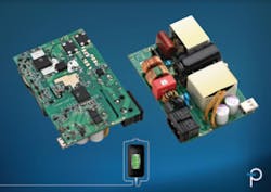
Power Integrations has published a new reference design for a USB Power Delivery (PD) charger with exceptional performance and very low component count. Based around the company’s new InnoSwitch3-PD PowiGaN flyback switcher and HiperPFS-4 PFC controller ICs, the DER-937 report contains the power-supply specification, schematic, PCB layout, bill of materials, detailed magnetics specifications, and performance data of a power-factor-corrected (PFC) 100-W USB PD 3.0 + programmable power supply (PPS) charger using only 117 components.
Aditya Kulkarni, senior product marketing engineer at Power Integrations, said, "This USB PD charger design reaches efficiency levels in excess of 93%, including input, PFC, and flyback stages. Its no-load performance is also excellent—the circuit requires less than 40-mW no-load input power at 230 VAC. BOM count is approximately half that of conventional designs, saving space, reducing design time, and simplifying component sourcing for high-volume manufacture of slim, ultra-compact OEM and aftermarket chargers."
DER-937 is available to download on the Power Integrations website at power.com/der-937.
Tech on the Beach: IEEE Symposium on VLSI Technology & Circuits in Cyberspace and Honolulu
Now in its 42nd year, the newly merged 2022 IEEE Symposium on VLSI Technology & Circuits is scheduled from June 13-17, 2022 in Honolulu, HI. The five-day hybrid event combines both live sessions, held onsite at the Hilton Hawaiian Village, with on-demand access to selected presentations and panel sessions.
In support of the theme “Technology & Circuits for the Critical Infrastructure of the Future,” the program will feature advanced VLSI technology developments, innovative circuit design, and the applications they enable. Applications range from artificial intelligence, machine learning, IoT, and wearable/implantable biomedical applications to big data, cloud/edge computing, virtual reality (VR)/augmented reality (AR), robotics, and autonomous vehicles.
The weeklong symposium is the microelectronics industry’s premiere international conference on integrating technology, circuits, and systems with a range and scope unlike any other event. In addition to the technical presentations, the symposium program will feature a demonstration session, evening panel discussions, joint focus sessions, short courses, workshops, and a special forum session that provides a focused discussion on a specific topic relevant to the symposia theme.
The symposium also will offer a series of workshop sessions that merge cutting-edge research with application information in areas that haven’t been covered in detail in the symposium technical program, and could serve as topics for future symposium sessions. They will be held in person during the symposium, as well as available as OnDemand recorded content following the conference.
Special events at the Symposia include mentoring events for Women in Engineering and Young Professionals, sponsored by the IEEE Electron Devices Society and the Solid State Circuits Society.
For further information, visit http://www.vlsisymposium.org.
Read more from the Power Management Series: This Week in PowerBites


