How the Tessent Streaming Scan Network Addresses Next-Gen IC Test
Reprinted with permission from Evaluation Engineering
There's a growing demand for next-generation ICs to deliver the extreme performance required for fast-evolving applications, such as AI and self-driving cars, putting tremendous pressure on the size of IC designs that now integrate billions of transistors. For the IC developer, larger and more complex IC designs and their associated complexity translate to a dramatic rise in the time and cost required to test them.
To address this issue and help silicon test teams manage these challenges, Mentor recently introduced the Tessent Streaming Scan Network functionality to its Tessent TestKompress software. This includes embedded infrastructure and automation that decouples core-level design-for-test (DFT) requirements from chip-level test delivery resources, enabling a no-compromise, bottom-up DFT flow that can dramatically simplify DFT planning and implementation while significantly reducing test time.
With full support for tiled designs and optimization for identical cores, it's ideal for increasingly large emerging compute architectures. Mentor’s Tessent Streaming Scan Network is a bus-based scan data-distribution architecture that enables simultaneous testing of any number of cores, helping shorten test time by enabling high-speed data distribution. It efficiently handles imbalances between cores, and supports testing of any number of identical cores with a constant cost. It also provides a plug-and-play interface in each core that simplifies scan timing closure and is well-suited for abutted tiles.
The solution consists of a series of host nodes in each design block that are networked together. Each host distributes data between the network and the test structures in the block. The software automates the implementation, pattern generation, and failure reverse mapping processes.
DFT engineers can fully optimize DFT test resources for each block without concern for impacts to the rest of the design. This helps to dramatically reduce the implementation effort. Along with optimized handling of identical cores, elimination of waste in the test data, and time multiplexing, this solution enables substantial reductions in test data time and volume.
To obtain an overhead view of the whole solution, we spoke with Geir Eide, Director, DFT Product Management, Tessent Silicon Lifecycle Solutions at Mentor. We talked about the solution set, how it addresses test issues, and the benefits to the IC designers and developers involved.
So can you start by giving us a quick explanation of the current situation?
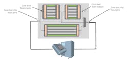
To just set the context, how typically digital ICs are tested today is that the most common SoCs consist of many building blocks, or cores. How we typically test the cores is that we connect all of the little memory elements inside the core into what we call chains, which is basically a mode that allows us to pump data into all of the memory elements and the design in an easy manner. And that's why in these diagrams here, you see all these green and gray lines here. That's supposed to represent what we call scan chains (Fig. 1).
So how this works is that these are connected one after another, and you do what we call shift data. So we kind of push data into these chains. And then we flip a switch and kind of turn into functional mode. Then we kind of run the chip in a very, very short amount of time. And we grab the results and shift the data from these chains out to the core. That's what's called scan test. It's been around since the '70s. That's still the basic concept we're using today.
Where things start to get more complex in these larger SoCs is that now a design typically consists of hundreds of these cores and building blocks. So you still need to connect at the chip level. And then you somehow have to distribute your pins to these different cores and touch the IOs at the die level, whether that's at wafer or package. But the additional challenge here is how you hook up all of these cores to the test point.
On the input side, you can, for instance, just broadcast them all to the inputs. But on the output side, you somehow need some sort of way of selecting. So if you have like 1,000 cores and you got 100 pins or 10 pins, you can't test all of these cores at the same time. Typically, you test some of them at the same time, and then you test others in sequence. The advantage is, the more you can test at the same time, the shorter the test time. But then, you're going to run out of pins at some point.
So part of the challenge then is to figure out which cores should I test at the same time? And we kind of typically put them in what we call groups, meaning that a group is a set of these cores that you test at the same time. Then you can kind of allocate five of those to this first core, and the other five to the second core, and do the same thing on the output side. You kind of make sure you connect five pins on one core and five pins to the other and see them to the top level. What we see more of is more nested cores where there's a core inside a core inside a core.
Can you elaborate on the core issue?
You got one big graphics core that goes on every chip. But inside the graphics core, you have other standard elements. And these standard elements have standard elements, right? So you get these more complex, multiple levels of hierarchies. Now, while the designs grow in size, we typically do not see an increase in the number of pins you can use for tests. If anything, that number is going down. And that's because your average SoC, whether it's something that goes in your phone or your computer or your car, tends to also have more and more of these high-speed pins, like USB ports and things like that.
Those pins are typically not allowed to be used for tests, because when you, for instance, throw in additional circuitry like a multiplexer, then things slow down. And test people have to stay away from those pins. So more and more data has to go through the same number of pins. Just to touch on one more thing here, we see, especially for chips that go into AI applications, huge numbers of identical cores. So many of these AI accelerators are used in parallel, massive parallel processing. And there are designs here that have thousands of exactly the same core.
In that case, you would like to leverage the fact that they are identical, because then you want to leverage that you can send all of the test data in at once, and just spread that out to all of these 1,000 cores. I don't have to test them, test one core after the other and kind of reload the same data into the chip. You should leverage the fact that these are identical.
So, these are some of the things that cause challenges for testing and for this way of dealing with hierarchical designs that we talked about. And kind of the main challenge here is that when we get more and more cores and levels of hierarchy, this design—hooking everything up, so the plumbing or the wiring, if you will—becomes challenging, especially because the decisions on how you hook everything up, you have to do that as part of the design process.
For example, looking at your house, you have to plan all your wiring or plumbing before you put the walls in place and start painting, because at that point, if you change your mind, you kind of have to pull the walls back out and start over again. It's kind of the same thing here.
For instance, if early on I say that, "Okay, I want to test this core and that core at the same time," then the problem with that is that after you've done with all the wiring and later, after you taped out and you start to generate the tests that you're going to apply in manufacturing, you notice something. You see over to the right here that you test these two cores at the same time. But it turns out that one is taking much more time than the other. So, then, there's kind of wasted resources here that you're stuck dealing with.
So you could fix that again, if you kind of tore out the walls and you decided, okay, I want to allocate more. Instead of hooking up five pins to one core and five to the other, I want to give the small guy just—sorry—three pins and the other one seven. But now you kind of go back and forth and it's more. Again, you have to tear out the walls and kind of go back and also change the cores. And that's very resource intensive.
Also, this approach that we are looking at here, for instance, doesn't really do anything for all the identical cores. That's because now. yes, you can broadcast the same data on the input side, but you still need to kind of observe all of... at least, you need to observe something from each of these cores here. If you got the 1,000 cores, you need at least 1,000 output pins to test all of them, or you have to again divide them into multiple groups and test them more sequentially.
Right. Now, one of the things that we're seeing in SoCs is the impact of migration and convergence. We're almost seeing a lot of the problems that board developers had back in the day now happening at the chip level.
Yeah. And I think in a way, it goes a little bit back and forth. I think there are times where things that were dealt with at the chip level start showing up at board level. But yeah. No, it certainly is because now that's kind of been the trend. I mean, that's why an SoC is called an SoC, right?
Right.
We kind of first saw this trend maybe 10 years ago when you started to go from just testing the entire chip as one blob to then dividing it into cores. And when you started to do that again, you didn't pay too much attention in the wiring to just be able to at least deal with one core at a time. That was very effective and kind of similar to in the board world. Years ago, there were only so many chips on the board. But then, all of a sudden, that starts to explode, right?
And heaven forbid you have to re-spin it.
Exactly. So some of the basic concepts are the same. And you can argue that some of the solutions that we're getting to here are actually some of the same as well. So again, the problem that we're trying to address is kind of the complexity of the electrical wiring in our house, if you will. And so today, there are really two solutions. Either you plan it very straightforward and say, "I'm going to treat all of the cores the same, and they're going to get five pins each. I'm going to test no more than five at the same time," type of thing. Or you can tear out the walls and go back and forth and spend much more time.
The benefit is you've reduced your manufacturing test costs. But, again, you have to spend more engineering effort into it. So there's this tradeoff that people deal with.
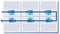
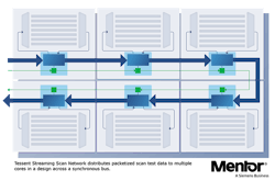
What we're introducing is something we called a streaming scan network, or SSN, which is a different way of sending test data, distributing test data across the chip. The idea is what you see in Figure 2. Instead of directly connecting the top-level pins to each core, so you kind of got this spaghetti of wiring from the chip-level pins to all the cores; there's a dedicated bus. The bus basically connects on the top-level pins to one core at a time. You see, it connects to this blue box that's inside each core.
What this blue box does is that you send data as packets on this bus, and each little box here understands what data actually is going to be used for this core. So we send data, let's say in a stream of packets on the bus, and each node is smart enough to say, "Yep, those bits, those are mine. I'll grab those." And then they also know when to put data back on the bus.
What about layout and space and the like? How much complexity does it add to the overall solution?
Well, the neat thing here is that from a layout point of view, this is much easier in the sense that rather than having all of the wires at the chip level that's spread out to all the cores, you're now creating a network that goes from one core to the next.
With tile designs, there is basically no top-level routing. You just put one core to the next and squish them together, so to speak. So if you need to connect something from one core and over to the third core over here, you have to kind of go through the core in the middle. So from a routing perspective, this alleviates a lot of the potential routing transition that you see with kind of the more traditional to pin methodology that most people are using today.
The other thing that is really neat about this is it decouples the core and the chip level. It used to be that when you determined what the test structure should be on the core, you really had to think about what happens when you put that core in a chip. So you need to know "How many pins do I have at top level?" "How many cores do I want to test in parallel?" Because that determines the chip-level requirements, which kind of impacts what you do at the core level. So everything is kind of dependent.
Here, that no longer matters. This width of the bus here, the size of the bus, is completely independent of what happens at the core level. So the guy who designs the core, he can do his thing without even talking to the guy who puts everything together. That's the secret sauce here, because that's also important when again, with this Lego principle, where this one piece of this one core is going to be used in maybe 15 different chips, this graphics core. Even though it's the same company, even though it's not Arm designing stuff that goes to some other company, even if it's within the company, people reuse stuff quite a bit.
Cores can be reused.
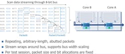
Exactly. And not only now, not only the cores, but also all of the test structures don't have to be re-tooled and re-modified based on which chip the core goes into. As an example, Figure 3 shows a very simple design with two cores, core A and core B. What's happening here is that core A, we say we have five what we call scan cells. That means that you have five independent signals that you need to connect to be able to send test data into the core. And for core B, it is four. The number of pins that you use for test access really depends kind of on the core itself. Typically, you want more pins, which makes the test time shorter. So think of it as kind of a rectangle. You can make it narrow and long, or you can make it short and wide.
In this case, typically, if you were to test core A and core B at the same time, you would have to have nine pins; nine pins to test the core B. Sorry, four for core B, five for core A, if you wanted to send data to them at the same time. We have this SSM bus, which in this example is eight bits. It could be any number of bits depending on the design. But in this case, we picked eight just to make it more interesting, since we need nine bits of data to be able to start sending data into the core.
So, what happens is that we send data, what we call packets, a term used in network protocols and Ethernet protocols. And kind of the idea here is somewhat similar. A packet represents all of the data you need to do one of these smallest type of test operations on a chip. So, to just send one set of data to all of the cores, that's one data. And in this case, one packet is nine bits corresponding to the five channels on core A plus five on core B.
And that's what all these letters mean inside of the packet. It means the first bit of data for core A is bit one for core A, and so forth. What you see here is this packet kind of wraps around the bus. So for this first packet, bit zero for core A is this the first bit on the bus. Then, the second bit for the second packet, you notice things rotate.
The clever thing about these light blue boxes here, what we call the host nodes, is where the secret sauce is. Rather than just having this kind of dumb, hardwired connection from the top-level pins to the cores, there's like a little bit... I wouldn't go as far as calling it intelligence, but these host nodes have to be smart enough to understand that this bit belongs to me and, then, this bit belongs to me. Then the decision of the data that they have to pick up is kind of in different locations. So they need to know exactly where, and when, is the data on the bus that I need to use?
And similarly, for the output response here, those same time slots that I used to provide stimuli for the core are also used to capture the output response. As this packet moves across the bus, once that data is consumed, it's picked up by the host; before that packet moves on the bus, it gets replaced. That input data for the core gets replaced by the output data.
So, the idea here is that you can now test lots of cores at the same time, even though you don't change the number of pins you have at the chip level. And again, you don't have to worry about how many pins you have at the top level versus what's happening at the core level. So it's a decoupling of your core-level requirements and your chip-level requirements. That's the secret sauce here. And how that is enabled is kind of the magic that's in the circuitry and in what we call hosts.
Now, the other thing that's very neat here is this idea of packetized test. We didn't invent the idea of a packet. There are other companies that have... I'm not aware of any other commercial solutions for this. Intel, for instance, did publish a paper on an approach that also uses packetized tests. But the challenge that they ran into is how they can tell what data a core should have rather than just what we call payload; the packets also contain an address. So it's like an address and data. Each packet says, "I belong to core A. And I belong to core B."
What we did instead is that something I haven't talked about—it's this green light and these small green boxes. This is like the programming of the host. That basically is how you set up the host, to say that for the data that's going to be sent to me soon, I'm going to pick up every 27th bit, or whatever the right number is. And that programming is done once per pattern set. Then, after that initial programming, everything is payload.
That also means that all these decisions of what do you test in parallel and what do you test sequentially are not done hardwired during the design. And again, you can make those decisions after you have painted the walls in your house, to go back to that analogy.
Got it.
In addition to the fact that you can kind of forget about things... Not forget about things, but how the core-level configuration and the chip-level configuration are independent. What makes that possible is also that normally, with a traditional approach, when you test multiple cores in parallel, which is when we're done pumping test data into the chip, and we run it in functional mode for a little bit—that's what we call capture—it typically has to happen at the same time.
So, if the amount of data we have to pump in is different, you again deal with this padding. And the reason why capture has to be aligned is that a lot of these signals that tell the chip whether you are in functional mode or in this test mode are generated at the chip level. Whereas with our approach, all of those signals are generated by that host. And that allows us to kind of not have to do everything aligned or in sync. It can be done more independently.
The other thing when we talked about the packets here—again, it's a previous example—I said a packet in this case would be nine bits because we got five pins on one and four on the other. What we can do is that if it turns out that core A requires much less data than core B, rather than send it five bits per packet, we can send it, say, three bits per packet and allocate more data to core B. If that makes more sense, that would kind of make them finish at the same time, which is something that this technology can do automatically. Rather than giving each core as much data as it has pins, if it doesn't need that much data to begin with, we can kind of automatically throttle or kind of reallocate the data stream.
Imagine if you have two faucets and two buckets, and you try to take a shower and use the sink at the same time, you don't have enough water pressure. And if you're trying to fill two buckets that are of different size, you're turning one faucet a little bit and having less water go into the small bucket. That's kind of what we're doing here as well. So this again means that not only is it easier for the guy who implements things, but you also have these things that take care of the test cost aspect.
About the Author
Alix Paultre's Archive
Editor-at-Large
Also check out Alix's main author page for his latest articles.
An Army veteran, Alix Paultre was a signals intelligence soldier on the East/West German border in the early ‘80s, and eventually wound up helping launch and run a publication on consumer electronics for the US military stationed in Europe. Alix first began in this industry in 1998 at Electronic Products magazine, and since then has worked for a variety of publications in the embedded electronic engineering space. Alix currently lives in Wiesbaden, Germany.
Also check out hjis YouTube watch-collecting channel, Talking Timepieces.


