Acoustic Solution for Bonded Wafer Voids
When infrared technology wasn t enough, pulsed ultrasound found the cause of leaky MEMS tubes.
An early and critical step in microelectromechanical system (MEMS) production is the bonding of two silicon wafers. The success of later processing steps usually is heavily dependent on the quality of the bond between the two wafers. When yield begins to decline for unknown reasons, the root cause may lie in the wafer bonding operation.
This suspicion arose during early/prototype production of MEMS density and flow meters at Integrated Sensing Systems (ISSYS). ISSYS designs and develops high-performance MEMS-based products that fit the smallest sizes, are biocompatible, and resist corrosion.
The density and flow meter is designed for very accurate measurement at low flow rates. When a liquid sample flows through the MEMS, it sets up a vibration whose frequency is specific to the concentration of the sample, such as the concentration of methanol in water in a direct methanol fuel cell system, the concentration of a drug in an IV line, or even the presence of air bubbles in an IV line. The resonant frequency is proportional to the density or chemical concentration of the liquid flowing in the MEMS.
On one of the silicon wafers, a number of U-shaped channels are plasma-etched, varying in depth and total length and having deep vertical sidewalls. The two wafers are first direct bonded, then annealed. After processing and removing most of the bulk of one wafer, these channels will become silicon resonating microtubes through which the liquid sample will flow. The wafer pair, after silicon thinning, is bonded to a glass wafer to which capacitor plates have been attached.
By sensing the frequency of vibration and the capacitance, the MEMS sensor identifies the concentration. The sensors are very accurate and very fast. They measure density or concentration to an accuracy of 0.0001 g/cc and resonate at 15 kHz, meaning that, theoretically, data can be obtained in 1/15,000 s although the real speed is slowed by microprocessor speed and other factors.
During production, the silicon tube assembly is vacuum packaged before being connected to an ASIC. Early production problems indicated that leaks were occurring in the U-tube channels. The channels themselves are from 50 to 500 microns wide, 100 microns or more deep, and up to 5 mm long.
Although it was clear that leaks were occurring, the mechanism creating the leaks was not known. But since voids are common anomalies in the bonding of silicon wafers, they were the first choice for investigation.
Two common causes of voids between bonded wafers are SiO2 particles and aerosols, both of which typically arrive on a wafer surface by airborne routes. If a void is caused by a particle, the diameter of the void is closely related to the diameter of the particle. But in the ISSYS application, a void might be very tiny and still result in a leak.
The first step was to attempt to find the voids in the bonded wafer pair via infrared microscopy. This attempt was unsuccessful, perhaps because the voids were too small for this technology.
Next, ISSYS shipped a number of bonded wafer pairs to the applications laboratory at Sonoscan. Acoustic microscopes pulse ultrasound into a sample, and the return echoes reveal internal features, including defects. So looking acoustically for voids seemed like a good starting point.

For any acoustic microscope application, the return echoes typically are gated on a particular depth of interest, meaning that echoes arriving before or after the gated time are ignored. A bonded wafer pair is structurally very simple, because, assuming that there are no cracks within the wafers themselves, the single depth of interest is the bond line between the two wafers.
The pulsed ultrasound is reflected only from an interface between two materials such as between epoxy and silicon in an IC package or between silicon and air in a bonded wafer void. It is not reflected from homogeneous materials without defects. If the two silicon wafers are well bonded and without voids or other defects, there will be no echoes at all from the depth of interest, and the acoustic image simply will be solid black.
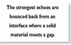
While the VHF and UHF ultrasound used in acoustic microscopes are reflected from any internal material interface, by far the strongest echoes are bounced back from an interface where a solid material meets a gap such as a void. Acoustically, bonded silicon wafer pairs are easy to image because the homogeneous silicon transmits sound easily while the voids give maximum reflection, resulting in pixels that typically are bright white in the acoustic image. Voids between bonded wafers are likely to be very thin, but the reflection from the voids is nearly total even if the void or gap has a thickness between 100 • and 1,000 .
Voids between bonded wafers can vary tremendously in area, and the ISSYS engineers were concerned that a void could cause a U-tube to leak. The leak could be caused either by a void 5 microns in diameter or a void 5 mm in diameter.
What mattered was that the void was adjacent to the tube. Voids located far from the tubes were not a threat. But voids close to but not impinging on a tube also could be a problem because they could cause the tube to rupture at low pressure.
The acoustic microscopes in the Sonoscan lab are capable of resolving voids down to 5 microns in diameter, which matched the smallest voids that ISSYS was interested in.
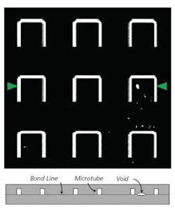
In the acoustic images, the U-tubes and voids were both bright white because they are both gap-type features that reflect ultrasound strongly (Figure 1). The images also showed that the size of the voids varied and that some of the voids were adjacent to U-tubes.
Following the confirmation of the suspected failure mechanism by the acoustic imaging of this first batch of wafers, ISSYS engineers fine-tuned the annealing temperatures of the wafers and made changes to the cleaning sequences used before bonding. Acoustic imaging of additional wafers showed that these process changes were successful: The voids became less frequent and then ceased altogether.
About the Author
Tom Adams is a freelance writer and photographer who has authored more than 500 articles for semiconductor and microelectronics trade magazines. Sonoscan, 2149 E. Pratt Blvd., Elk Grove Village, IL 60007, 847-437-6400, e-mail: [email protected]
FOR MORE INFORMATION
on acoustic microscopy
www.rsleads.com/609ee-185
About the Author
Comment About the Article
To join the conversation, and become an exclusive member of Electronic Design, create an account today!

Leaders relevant to this article: