Test Methodology Using PXI and High-Speed Digital I/O
A typical pattern generator-style test methodology (test vectors) often is used when testing digital devices to verify functionality, register access, and determine that read/write data meets design criteria. The tried-and-true method of generating a pattern, reading back device response, and then parsing the response waveform for a specific pattern match will yield a solid test system.
However, what if you need to test not only the passing results for expected vectors, but also the timing of the result vectors? And what if you need to loop these timing tests across several parameters such as input voltage, clock speed, and source current? And of course, you may be testing hundreds of register combinations to fully verify your new design.
Now we are defining a characterization system, and using a traditional methodology typically will yield long test times and slow loop iteration rates. This can turn minutes into hours per test and hours into days per loop parameter. And adding scope triggering and post-capture signal analysis for generating accurate timing measurements increases code complexity and requires more processing time to generate the data needed for the end result—a full range of sweep data per test consolidated into a meaningful report.
To accomplish these tasks, G Systems architected an I2C characterization/validation system with a new and different test methodology using the hardware-compare features of a PXI 100-MHz high-speed digital I/O module. Hardware-compare of generated data to acquisition data is a hardware-based simultaneous test using software-defined compare samples. The result is an array of sample errors and their sample location in your test-vector waveforms.
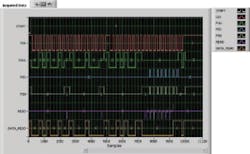
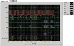
Figure 1 illustrates several lines of generation data (START, CLK, FULL, MID, MIN), the hardware compare sample locations to test (READ), and the acquisition line (DATA_READ).
By using hardware compare, you already have the failure locations noted without analyzing the acquisition data in a separate step. And since we know what our sample clock is and where any particular sample edge is in our test vector, we can calculate digital timing data by defining reference points for comparison purposes.
For example, in Figure 1, we are expecting to read back 0x01 from a particular register to which we have already written data. In this figure, the result is pass since the data read matches the expected data. But if we also wanted to know exactly when the last data bit went active high, we could cover an area of samples from 9,000 to 10,000 in the hardware compare data while ignoring samples from 7,000 to 9,000 and expect a fail result.
The last point of failure in the array would be when our expected data shifted from a zero to a one. By adding one (+1) to that last failure sample location, we now have the location of the first edge shift to valid data.
Referencing this location to the falling edge of clock (CLK) at sample 9253 (test against the known sample location defined in the saved waveform) and multiplying by the sample clock interval give us the timing spec from the falling edge of a serial clock line (SCL) to the valid serial data line (SDA) response from the device. This result corresponds to the propagation delay in the device output circuitry after a falling clock is detected and shifts as parameters such as device power (Vdd) or logic-level voltages change.
This particular test system yields timing results with 10-ns base resolution, a maximum of one sample clock error, and fast loop execution times using the hardware-compare methodology and automated dynamic waveform modification for shifting data edges in real time. Executing tests with a COTS test executive and a simple database enabled datalogging and reporting and provided easily coded looping structures for characterization parameters.
Full characterization sweeps across hot, room, and cold temperatures take only a few hours, which is due mostly to the settling of soak temperatures rather than the actual testing. Characterization with similar bench hardware, automated vectors, and semi-automated tests using the traditional approach could require days or even weeks to run, not counting the extra effort to manage data collection and develop reports necessary for analyzing the characterization data.
System Architecture
Hardware
A PXI-based system design was chosen for high data throughput, high speed and timing synchronization for digital signals, and tight integration with development tools. At the core of the characterization system is a high-speed digital I/O module. With its 100-MHz sample clock and programmable voltage generation and acquisition, G Systems was able to fully characterize I2C digital timing over voltage input high (Vih), voltage input low (Vil), and device clock speeds.
Pull-up drive current also was programmable using multiple drive pins with varying current-limiting resistors on the test board. These SDAs could be driven simultaneously while in the high-impedance state when not in use with per-sample resolution, which was effective in measuring device data rise and fall times and ensuring proper device response.
In Figure 1, these lines are noted by FULL, MID, and MIN. The SCL was driven with a single generation pin at device clock rates of 100 kHz to 1 MHz. This device clock was generated using the full sample clock range to provide 10-ns step resolution for the timing tests.
All timing results were valid to within ±10 ns with the current software and hardware. One improvement idea was to use the data delay feature of this particular module to increase the resolution even further to ±40 ps, sacrificing larger loop iteration times. But that has not been determined necessary or implemented at this time.
A 60-MS/s digitizer was used for capturing actual device response waveforms. Two source-measurement units controlled Vdd and analog stimulus to secondary function pins outside the I2C specification. A 6.5-digit DMM was used to provide higher resolution measurement of current drawn through Vdd and as a bench resource for determining device voltages.
Two expansion slots are available for any future switching, data acquisition, or other instrumentation needs. A digital I/O breakout board was used in prototyping the DUT connection interface with terminated digital I/O, input power connections, and a solder board-style interface.
Software
A modularized system architecture was designed to manage the instrumentation, test step execution, data collection, and reporting. All instrumentation control and parametric and digital timing tests were developed using custom software with test sequence automation, datalogging, and reporting handled by the COTS test executive.
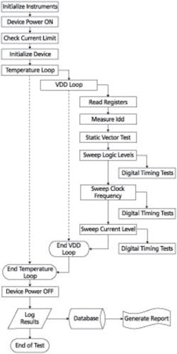
Since the characterization system is geared toward primarily testing I2C devices, but not limited to those devices, this architecture lends itself to coding new validation tests with predefined test steps and saved test templates using the features of the test executive development environment. Tests are tailored to specific devices by simply adjusting a few input parameters such as device ID, address, register, and data bytes. These tests then are looped over varying input parameters such as Vih, Vil, Vdd, temperature, and device clock as shown in Figure 2.
The total test time increases per swept parameter and control loop parameter. Consequently, reducing the overall test-step execution time is critical in minimizing characterization run times.
What is not shown in Figure 2 is the waveform sweeping necessary to shift signal edges during each of the digital timing tests. Depending on device performance and the specific test pattern needed, these waveform sweeps could number from one to a few hundred samples before the correct trigger event occurs. The new test methodology significantly reduces per iteration execution time, which decreases the entire characterization loop execution time.
One core design challenge was to build tests based on engineering design data and test vectors. This was accomplished by using a waveform editor to import value change dump (VCD) files, which are exported Verilog vectors formatted into text. Once imported, the signals are modified to match the DUT test board and scaled to 100-MHz sample clock timing. Then the vectors are saved into a digital waveform file ready for use with the test steps.
Another aspect of this design approach is using software to programmatically modify the contents of the digital waveform on-the-fly. This design approach facilitates shifting either SDA or SCL waveform edges, inserting adjustable width spikes in the data, and running specific pattern tests using predefined or programmatically changed hardware compare locations.
Utilizing the digital I/O module’s hardware-compare feature was critical in achieving fast test times and loop execution throughput. Instead of the typical scenario of generating data, acquiring data, and then searching through the acquired data for a pattern match, hardware-compare allows for direct comparison of data during acquisition.
The hardware-compare function provides an array of failure sample locations and the failed data pins. Referencing vectors in terms of sample locations to the minimum sample clock resolution vs. device-specific bit locations presented a more user-friendly way to define input test parameters.
Having the ability to visualize expected input and actual device response data before running a test helps the engineer in troubleshooting test parameters and analyzing any failures. Sample referencing also made use of previous code for shifting edges in defining data read and write test steps as opposed to building entire test vectors from scratch.
With programmatically writing a digital I/O pattern, the engineer must wait until generation and capture to see the results, make adjustments to code or vector timing, and then rerun for a valid pattern. The time saved in development was significant, and the code was much easier to maintain and reuse.
Conclusion
The finalized characterization system measures I2C digital timing and analog parameters to validate that new designs and packaged silicon meet the latest design specifications. Ensuring specifications are met with the ability to show hard data helps prove the device can function correctly within the customers’ new mixed-signal designs such as cell phones, computers, and proximity sensors.
Another benefit is the capability to test return material authorization (RMA) requests to determine any root cause of failures and compare returned device test data to initial test data for any discrepancies. This helps capture latent design defects or validate there were no issues with the device design/performance and look for faults elsewhere in the user application. The result of such action could save millions of dollars in revenue lost to device recalls.
All analog parameter and digital timing sweeps can be tested on a device over varying temperature ranges within a few hours as compared to a few days or weeks when performing similar tests in a semi-automated system. This greatly reduces time-to-market and quickly closes the design validation loop for the product design engineering team.
About the Author
Rick Garza is a staff project engineer at G Systems. Before joining the company, he held positions as a staff engineer at VI Technology, senior test engineer at Navini Networks, OEM manager at Test Technology Associates, test engineering manager at Xetel, and senior test engineer at Genrad. Mr. Garza received a B.S. Electronics Engineering Technology degree from Texas A&M University and an M.B.A. in business computer information systems from the University of North Texas. G Systems, 1240 E. Campbell Rd., Suite 100, Richardson, TX 75081, 972-234-6000, e-mail: [email protected]
About the Author
Voice Your Opinion!
To join the conversation, and become an exclusive member of Electronic Design, create an account today!

Leaders relevant to this article:


