SEMICON West and the co-located Test Vision 2020 convene next week in San Francisco, where makers of automated test and inspection equipment, components, software, and related products will have a forum for describing their latest technologies. Traditional ATE makers including Teradyne and Advantest will be exhibiting, with the latter highlighting a memory test system, optical port module, and IoT test on the V93000 platform.
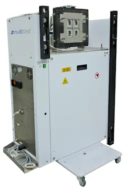
Xcerra will also be participating, with its Multitest subsidiary offering two presentations at Test Vision 2020. Multitest will describe RF and PHY testing requirements for wireless IoT devices and final-test solutions for wafer-level chip-scale packages. The company’s most recent new product is a magnetic rotation stimulus (MRS) module, enabling additional sensor-test capabilities on the MT9510 handler as part of the company’s MEMS/sensor test product line.
In addition, Marvin Test Solutions said it will show the TS-900 family of semiconductor test solutions, which are based on the PXI modular platform while providing users the features and capabilities associated with “big iron” ATE. Also expected to showcase PXI-based systems is National Instruments, which offers the STS Semiconductor Test System.
Other companies who have offered specifics about their plans for the show range from software vendors to component makers. In the latter category, Pickering Electronics, a manufacturer and distributor of instrumentation-grade reed relays for ATE, RF switching, and other applications, announced it will showcase new high voltage micro-SIL reed relays at SEMICON West 2015.
Pickering says its new Series 119 range for up to 3 kV is the industry’s smallest high voltage single-in-line reed relay now available. Intended for voltages higher than standard small SIL relays can handle, Series 119 relays are suitable for cable testers, mixed-signal ATE, and other applications where high-voltage capability is required.
As for software, Optimal+ will be on hand to exhibit its latest offerings, including Optimal+ 6.0, which offers real-time, big-data analytics from new-product introduction (NPI) to high-volume manufacturing (HVM). David Park, vice president of worldwide marketing, said in a recent phone interview, “Our solutions transform manufacturing test data into actionable intelligence that improves yield, quality, and productivity with full supply-chain visibility.”
Park added that the company’s technology improves yield recovery, quality, and efficiency in high-volume production but that customers have asked that Optimal+ extend its data-management and analytics capability to NPI and characterization.
To that end, the company last month introduced EXACT (derived from Extreme Analytics and Characterization), which is specifically designed to address analytics challenges for both HVM and NPI. For the latter, Park said, it “…delivers next-generation capabilities for the collection and management of characterization data with powerful data-analytics and advanced report generation.” Specifically, he said, EXACT can help manage “dirty” characterization data, providing a sandbox in which characterization data can be cleaned up and leveraged into the HVM process.
KLA-Tencor will also be on hand at SEMICON West, and it will likely highlight two new systems that support advanced semiconductor packaging technologies: CIRCL-AP and ICOS T830. Designed for characterization and monitoring of the diverse processes used in wafer-level packaging, CIRCL-AP enables all-surface wafer defect inspection, review, and metrology at high throughput. The ICOS T830 provides fully automated optical inspection of IC packages, leveraging high sensitivity with 2D and 3D measurements to determine final package quality for a wide range of device types and sizes.
In a recent phone interview, Prashant Aji, head of marketing for the company’s SWIFT division, commented on packaging trends. Driven by mobile devices, he said, packages are shrinking, with an increasing use of wafer-level packaging, and the industry is pushing to cut packaging costs. In addition, packaging is increasingly shifting to OSAT companies.
These trends are altering the semiconductor manufacturing process. The move to wafer-level packaging, Aji said, inserts between the traditional wafer-level frontend processing and the backend wafer-cicing and packaging process a new middle-of-the-line or “middle-end” stage, involving wafer-level TSV (through-silicon via), RDL (electrical redistribution layer), and bumping operations, with bump size and pitch decreasing, RDL line/space shrinking, and use of TSVs increasing. In addition, Pieter Vandewalle senior director of marketing for KLA-Tencor’s ICOS Division, said that demands for longer battery life in mobile devices means less space for packages.
Read our August print issue for more on the new KLA-Tencor products and technologies. Meanwhile, see these related articles for more on automated test and inspection and related topics:
- Multitest launches magnetic sensor test module for MT9510
- Pickering to showcase new reed relays at SEMICON West
- Optimal+ 6.0 offers real-time, big-data analytics from NPI to HVM
- Avoiding test escapes— when is good really good?
- KLA-Tencor addresses advanced semiconductor packaging
- Keynotes, TechXPOT sessions set for SEMICON West
- Using EDT Test Points to reduce test time and cost
- Packaging, test issues up for debate at SEMICON West
And read our full ATE coverage here.
About the Author

Rick Nelson
Contributing Editor
Rick is currently Contributing Technical Editor. He was Executive Editor for EE in 2011-2018. Previously he served on several publications, including EDN and Vision Systems Design, and has received awards for signed editorials from the American Society of Business Publication Editors. He began as a design engineer at General Electric and Litton Industries and earned a BSEE degree from Penn State.
Voice Your Opinion!
To join the conversation, and become an exclusive member of Electronic Design, create an account today!

Leaders relevant to this article:


