Forging a bright future for IC and package quality

Vendors are taking a variety of approaches to boosting semiconductor quality and reducing time to market. Offerings range from instrument modules in PXI and LXI formats to complete test and related systems—and finally on to software that manages “data lakes,” applying AI/machine learning for analytics. Application areas are similarly varied—extending from analog to high-speed digital and on to RF, with wireless and IoT devices gaining considerable attention. SEMICON West, scheduled for July 11-13 in San Francisco, will provide companies an opportunity to highlight these products and technologies.
National Instruments will be focusing on wireless technology at SEMICON West. “The two largest trends in wireless devices in 2017 are the approaching finalization of the 802.11ax specification layer and continued breakthroughs in 5G technology,” said Ben Robinson, product marketing manager for the company’s automated test team. “Testing 802.11ax introduces challenges like more stringent error-vector-magnitude measurements. In addition, new 802.11ax multi‐user OFDMA and MIMO technologies drive new measurement requirements like access-point power correction. In parallel, 5G also introduces additional design and test challenges to mobile radios. The 5G new radio specification will utilize wider bandwidth and MIMO technologies for high-throughput data transmissions—and require higher performance instrumentation as a result.”
Paul Bovingdon, product manager, Pickering Interfaces, said, “The primary challenge facing the type of testing that we focus on—including shorts/opens, capacitance, and I-V test for transient charge trapping and SCPT (single charge pulse trapping)—is ever-increasing I/O counts. The problem with this is the issue of controlling many more relays simultaneously and doing it as fast as possible. This has led us to add sequencing circuitry in our switching systems that can be triggered by other hardware or software in the test system.”
Mike Dewey, director of marketing at Marvin Test Solutions, said, “We see ongoing demand/trends to lower the cost of test. Users are continuing to look for new and better ways to utilize the test resources they have; this is probably exacerbated by the emergence of IoT devices that are driving up volume but with the accompanying demand for lower ASPs.”
Jon Sinskie, executive vice president at Astronics Test Systems, said Astronics will be emphasizing system-level test (SLT) at SEMICON West. “Our customers now recognize the need to implement SLT into their manufacturing process and want to do so in an affordable manner,” he said. He cited several trends driving this need—new smaller nodes can increase the number of missed transistors during traditional testing, high-speed bus interfaces (such as LPDDR, PCI Express, and USB 3.0) require faster read/write turnaround times than can be achieved with traditional ATE, and new packaging techniques such as heterogeneous packaging are driving higher escape costs as multiple known good die are integrated into a single 2.5D/3D package. “We are working closely with chip manufacturers to build the right SLT solutions to meet their specific challenges,” he said.
SEMICON West exhibits
To address the challenges posed by evolving wireless technology, NI offers the PXIe‐5840 Vector Signal Transceiver (VST) (Figure 1), which the company will exhibit at SEMICON West. The VST, NI’s Robinson said, is the world’s first to achieve a 1-GHz bandwidth. It combines a 6-GHz RF vector signal generator, a 6-GHz vector signal analyzer, a high‐performance user‐programmable FPGA, and high‐speed serial and parallel digital interfaces into a single two‐slot PXI Express module.
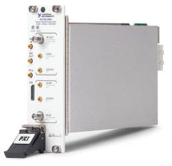
Courtesy of National Instruments
“With 1 GHz of bandwidth, the latest VST is ideally suited for a wide range of applications including 802.11ac/ax device testing, mobile/Internet of Things device testing, 4.9/5G design and testing, RFIC testing, and more,” Robinson said, citing a key takeaway for SEMICON West attendees: “NI has a platform that provides users with flexibility to address the upcoming test needs of new wireless connectivity standards, such as 802.11ax, even as they continue to evolve. With 1 GHz of instantaneous of bandwidth, the second-generation VST … is an essential instrument to test wideband mobile technologies based on 5G.”
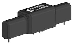
To help customers contend with high I/O counts, Pickering Interfaces at SEMICON West will highlight its soon-to-be-released Model 65-221 High-Density Modular LXI Reed Relay Matrix (Figure 2), Bovingdon said. “Originally designed to test semiconductors at wafer and package levels, the reed relay matrix solution combines our LXI modular matrix chassis (Model 65-200) with our new plugin matrix modules that provide access to all signal connections on 200-pin connectors. It is capable of supporting matrices with a Y-axis size of four and expandable in the X-axis range up to 1,536 in increments of 128. Users can specify as many or as few plugin modules (up to six) as required and can field-upgrade the chassis to extend the matrix when necessary. Another important feature is that more than 1,500 relays can be closed simultaneously for specific conditions for parametric testing.”

Courtesy of Pickering Interfaces
Bovingdon described Model 65-221 as part of a new range of LXI reed relay plugin matrix modules, which includes three additional plugin modules covering matrices of up to 768 x 8 in increments of 64 (Model 65-223), 384 x 16 in increments of 32 (Model 65-225), and 192 x 32 in increments of 32 (Model 65-227). “Each plugin provides a single or dual 128 x 4 submatrix with the capability to connect its Y axis to one of 12 or six analog buses (depending upon the plugin model type),” he said, thereby providing a high degree of flexibility in matrix configuration and making parallel testing much simpler.
“These plugin matrices also offer a built-in scan list of up to 5,000 predefined test sequence stores with triggering capability, providing users with the ability to set a series of predetermined sequences on a LXI instrument,” he added. “The sequences can be triggered by software or one of the six software-configurable triggers.”
Pickering Interfaces also will highlight its high-density PXI matrices, its two-slot USB/LXI modular chassis, and its Switch Path Manager signal-switching software at SEMICON West.
In addition, sibling company Pickering Electronics will highlight its lineup of reed relays, including three new series of high-voltage single-in-line (SIL/SIP) devices that all offer high packing density: the Series 119 micro-SIL relays are rated up to 3 kV. The company calls the Series 119 the industry’s smallest high-voltage SIL/SIP reed relays for up to 3 kV stand-off; they are suitable for cable and backplane testers and mixed-signal ATE.
The Series 67 and 68 reed relays (Figure 3) are available for up to 10-kV stand-off, 7.5-kV switching, with an option of either PCB or flying-lead switch connections. Similar in specification to the company’s established Series 60/65, these new relays are manufactured in a SIL/SIP format using former-less coils—dispensing with the more usual coil-supporting bobbins, allowing a smaller package than similarly rated devices.
Courtesy of Pickering Electronics
MTS plans to exhibit several products at SEMICON West this year, including the TS‐960e PXI Express semiconductor test system (Figure 4). “Introduced last fall at Autotestcon, the TS‐960e offers a cost‐effective, open architecture test solution for digital, analog, and RF applications,” Dewey said. “Leveraging Keysight’s PXIe RF instrumentation portfolio, the TS‐960e can address a wide range of RF test capabilities for WLAN, Bluetooth, cellular, EW, and RF transceivers—for both wafer and packaged test applications.”
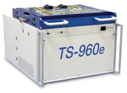
Courtesy of Marvin Test Solutions
The company also will highlight the Marvin Test Expansion Kit (MTEK) Series, which offers a tester upgrade solution for legacy semiconductor test systems. “PXI-based, the MTEK is a compact solution that is compatible with legacy test platforms, including Teradyne, LTX/Credence, and Verigy,” Dewey said (Verigy having been acquired by Advantest). “The MTEK can be configured to support RF, digital, and analog capabilities.”
Added Dewey, “Test engineers are looking for creative ways to extend the life of test systems with more capabilities and/or capacity. Low-cost ‘add‐ons’ like the MTEK Series provide one way to help accomplish this goal.”
MTS also has expanded its semiconductor software tools portfolio with the addition of the ICEasy Test Suite, Dewey said. The suite includes a library of test-development tools (including Shmoo and I‐V plotting) for creating test programs and characterizing devices; a software tool set for importing and converting STIL, WGL, VDC/EVCD, and ATP files to a Marvin Test Solutions digital instrument file format; and digital waveform edit/display tools. “The test suite interfaces seamlessly with ATEasy,” Dewey said. He concluded, “Open architecture test solutions like PXI (both hardware and software) are viable and compelling options for both new test needs and for augmenting the legacy/installed base of test systems.”
System-level test
At SEMICON West, Astronics Test Systems will highlight its new ATS 5034 system-level test platform. “This platform improves production efficiency and greatly reduces the cost of system-level test by processing up to 396 devices simultaneously,” Sinskie said. “The ATS 5034 SLT platform is ideal for testing the latest semiconductor devices for mobile, automotive, wearable, and industrial applications. Customers will benefit from the dramatically reduced footprint of the ATS 5034 SLT platform and the ability to test up to 5,000 units per hour.”
He continued, “For the past 20 years, we’ve provided system-level and burn-in testers that have tested more than 9 billion semiconductor devices globally. The ATS 5034 SLT platform offers a breakthrough in test technology that significantly improves yields by providing an affordable method for semiconductor manufacturers to implement 100% system-level test insertion into the production process. Customizable and adaptable, this versatile, modular platform satisfies a variety of manufacturing test functions including system characterization, validation, and qualification; system level test; and RMA/failure debug.”
Software for test-time reduction
On the pure software side, Optimal+ at SEMICON West will highlight version 6.9 of its flagship software—the first version that supports Hadoop for some key customers and that adds new capabilities for adaptive test time reduction for automotive customers, according to David Park, vice president, worldwide marketing.
When asked about key trends, Park said, “What we are seeing in all our customers is the move toward ‘data lakes’ to hold all of their data, not just manufacturing test data.”
Park continued, “The overall management of manufacturing data combined with AI/machine learning for analytics is a ‘must have’ capability to be a top supplier for end customers, and it is not a competency that can be maintained through internally developed tools. Commercial solutions are aggregating so much knowledge due to their growing adoption by customers that in‐house tools simply cannot compete with what is available in the marketplace. Similar to the universal adoption of EDA tools on the design side, it is just a matter of time before all semiconductor and electronics companies will adopt commercial tools for big-data analytics of their manufacturing operations, and the sooner that companies adopt these tools, the more competitive they will become.”
Packaging applications
And finally, Orbotech said it would be highlighting its Inkjet 600 (Figure 5), which provides additive printing for IC packaging production. Based on Orbotech’s DotStream Pro technology, the Inkjet 600 prints fine lines and uniform thin layers at any angle and on a range of materials. Its automatic measurement and scaling modes enable market-leading registration and accuracy, the company said, offering flexible, cost-efficient solutions for IC packaging applications, including tall, high-aspect-ratio 3D dams (ratio of 1:4); accurate isolation layers; and IC unit marking and serialization. The company announced in July 2016 that Amkor Technology had selected the Inkjet 600 to print high-aspect-ratio 3D underfill dams for new system-in-package products.
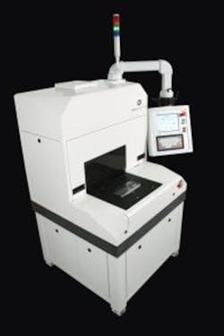
Courtesy of Orbotech
“The main new challenges since last year are improving our ability to print on new materials and new wafers, printing with new and varied types of ink, and increasing our 3D printing capabilities so that we can print higher dams,” said Hanoch Kopel, director of corporate business development, in a recent email. “A significant challenge we have overcome is the ability to print on various materials like silicon and electronics.”
Kopel concluded, “Orbotech’s expertise in 3D printing is our ability to print high-aspect-ratio structures and to print directly on the electronics and isolation layers of diverse substrate types, such as PCBs, silicon wafers, molded wafers, and metals.”
From NAND to IoT
Other companies haven’t detailed specific plans for SEMICON West, but Advantest is likely to highlight system-level test for the embedded-NAND market. Ken Hanh Duc Lai, marketing director, cites forecasts that mobile memory shipments could exceed 2 billion units by 2020, with a transition from embedded multimedia cards to the JEDEC-defined Universal Flash Storage (UFS).
“Memory IC makers need a class of tester that specializes in SLT of these devices while maintaining the reliability, low cost, and high-volume capabilities required for conventional memory testers,” Lai writes.1 “Advantest developed its T5851 SLT solution—part of the T5800 platform series—specifically to meet these needs, delivering cost-effective testing of UFS and BGA SSDs.”
Advantest also is likely to highlight IoT test, with an emphasis on improved time to quality (TTQ) by speeding the transition from design to high-volume manufacturing (HVM). “A new integrated ATE solution being embraced by several leading semiconductor suppliers utilizes engineering ATE that comprises the same hardware instrumentation, software environment, and DUT interface fixturing as the ATE used for HVM test,” writes Neils Poulsen, director of SoC business development.2 “This compatibility accelerates test-program development and bring-up, correlation, and release to HVM by leveraging the engineering efforts from the previous phases—resulting in reduced costs and improved TTQ.”
References
- Lai, K. H. D, “System-Level Test Essential for Fast-Growing Embedded NAND Market,” Go Semi & Beyond, May 4, 2017.
- Poulsen, N., “IoT Devices Require a New DFT Paradigm and Scalable ATE,” Go Semi & Beyond, Feb. 19, 2017.
For more information
About the Author

Rick Nelson
Contributing Editor
Rick is currently Contributing Technical Editor. He was Executive Editor for EE in 2011-2018. Previously he served on several publications, including EDN and Vision Systems Design, and has received awards for signed editorials from the American Society of Business Publication Editors. He began as a design engineer at General Electric and Litton Industries and earned a BSEE degree from Penn State.
Comment About the Article
To join the conversation, and become an exclusive member of Electronic Design, create an account today!

Leaders relevant to this article: