Optical Semiconductor Inspection Using High-Speed Machine Vision
What you'll learn:
- Line-scan vs. area-scan cameras.
- Key ingredients to the high-speed machine-vision system for inspection.
- How to synchronize the wafers with the camera.
Optical semiconductor inspection presents complex challenges, including the diminutive size of the target and proximity of individual dies in the wafer space. At the same time, the quality of wafer inspection results is critical due to the risks involved if requirements aren’t met. For these reasons, vision systems with exceptionally high speed and resolution capabilities can play an important role in semiconductor inspection.
CoaXPress high-speed, machine-vision area-scan cameras stream data directly to a backend machine for processing. The nature of semiconductor inspection requires robust image processors, such as graphics processing units (GPUs) and field-programmable gate arrays (FPGAs), as well as high-end and powerful central processing units (CPUs), depending on the configuration and required throughput.
What Makes Up the System?
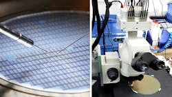
The machine-vision system is comprised of three major components: a high-speed camera, a microscope, and an air-bearing X-Y stage to safeguard Z-axis movement of the wafer. The camera is integrated with a Nikon LV-M microscope (Fig. 1).
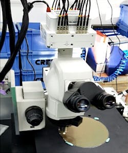
Both camera and microscope were mounted on an HybrYX air-bearing stage to isolate any movement in the Z-direction. The air-bearing stage helps to avoid any inconsistency in depth of field (DOF) of die that might skew the focal length of the lens.
For this test, the resolution of the sensor was reduced to 1920 × 1100 pixels with an exposure time of 100 µs and speed of 2500 fps to meet the inspection requirement. In addition, the air-bearing stage’s X-axis speed was set at 300 mm per second; the camera receives an external trigger signal from the system controller via a general-purpose input/output (GPIO) cable.
Camera and Wafer Synchronization
Synchronizing a single die unit in a two-dimensional moving table with the exposure time of the camera is a critical part of the setup. If accomplished correctly, the result will be consistent image analysis with a defined field of view (FOV).
The high-speed camera enables use of a GPIO cable to send external signals to the camera for trigger, sync, IRIG, and other functions. In this setup, the camera was synchronized with the speed of the table in relation to a single die unit, such that the trigger signal aligns with the exposure time of the frame. Alignment with the edge of the beginning of a single die within a wafer is thereby achieved. This precise synchronization of the trigger signal to the camera avoids a scenario in which the camera receives a trigger signal in the middle of a die.
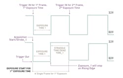
The trigger-in signal should be sent at the beginning of the falling edge of the frame when the sensor begins exposure—with two consecutive falling edges defining a single frame. A time between a falling edge and a rising edge is an exposure time. Thus, in the synchronization process, the falling edge of an exposure time is where a trigger-in and sync signal is sent to the camera via the GPIO cable.
The camera begins to capture footage at first edge of the die. Exposure stops when the camera sees the last edge of the die, or before the beginning of the next die. The first edge of the die is synchronized with the falling edge of the frame (the start of exposure time) and the last edge of the die is synchronized with the rising edge of the frame (the end of exposure time) (Fig. 2). The camera follows this task repeatedly, scanning the entire wafer.
As shown in Figure 3, the key takeaway from this mechanism is that the entire die in a wafer can be precisely scanned in a very short period of time by synchronizing the external signal with the camera to capture an image with intended FOV, perspectives, and contrast.
A well-designed machine-vision system will improve product quality, decrease inspection time, and reduce takt, which is rate at the process can be completed. For semiconductor inspection, the faster the cycle time, the more quickly inspection can be completed. This ultimately reduces overall process time and production costs.
In our test system, the implementation of the high-speed camera increased the manufacturing and packaging process significantly by increasing wafer-per-hour inspection from 1 to 2 wafers to 10 to 15. To further analyze the data:
- v = 300 mm/s
- d = 1600 px × 10 µm = 16 mm
- t = d/v = 16/300 = 53 ms/die
- Die per wafer = 1000
- Total time per wafer = 1000 × 53 ms/die = 53 sec ~ = 1 min
Assume there’s 100% overhead time due to software image processing. Cycle time per wafer goes from 1 to 2 minutes. The number of wafers processed by the camera and software per hour equals 30 wafers. This is 15 times more than ASML or similar systems can process per hour.
Replacing a line-scan camera with a high-speed area-scan camera reduces takt time and increases yield by increasing the amount of wafer range inspected per given time. In the past, line-scan devices have been credited for scanning a larger line range and post-processing stitched images. However, high-speed cameras can scan 1,000X more area than line-scan cameras, not to mention that the image is available immediately for processing without an image stitching process.
Conclusion
Machine-vision systems provide superior speed when implemented in semiconductor inspection, increasing quality of product and reducing takt and cost significantly. Previously, a line-scan camera was preferred to achieve relatively higher speeds by scanning larger surface areas and stitching lines to form a single frame. High-speed inspection of a larger surface area of a wafer can be achieved with a high-resolution area-scan camera, which scans significantly faster than a line-scan camera.
About the Author
Uma Gobena
Field Application Engineer, Vision Research
Uma has a degree in mechatronics engineering from Ryerson University in Ontario, Canada. He had six years of experience as a vision systems engineer before joining Vision Research in 2019.
Comment About the Article
To join the conversation, and become an exclusive member of Electronic Design, create an account today!

Leaders relevant to this article: