IBIS Modeling (Part 2): How to Create Your Own IBIS Model
This article is part of the Test & Measurement library series: Simulate Your Way to Design Success with IBIS Modeling.
Members can download this article in PDF format.
What you'll learn:
- Defining a basic IBIS model.
- The premodeling process.
- Setting up and simulating with LTspice.
- Determining rising and falling waveforms.
- Ramp data extraction using LTspice.
- How to build an IBIS model.
Simulation plays a key role in building any system. It allows designers to foresee problems and prevent time-consuming and costly revisions. The goal is always to do it right the first time! In the case of simulating high-speed digital interfaces, a simple PCB trace could affect the quality of the signal if not designed properly. In signal-integrity simulations, an IBIS (input/output buffer information specification) model is used as a representation of the device’s digital interfaces.
As discussed in Part 1 of this article series, IBIS is a behavioral model that describes the electrical characteristics of the digital interfaces of a device through tabulated current vs. voltage (I-V) and voltage vs. time (V-T) data. It’s important for the IBIS model to be as accurate as possible and not have any parsing errors to avoid any issues when using it later.
In addition, there should be an available IBIS model for each part or device that has a digital interface. So, whenever customers need one, they can download it directly from the manufacturer’s web page. However, this is not always the case.
For IBIS model users, one problem they always face is model availability. When the part they chose for their design doesn’t have an IBIS model, this might delay product development.
The best source for an IBIS model is from the manufacturer itself; however, it’s still possible for the user to create IBIS models. This article introduces a way to create the most basic IBIS model derived from a Spice model using LTspice. The following sections use the specifications from the IBIS Modeling Cookbook for IBIS version 4.0 to discuss LTspice simulation setups. Validating the IBIS model also is tackled utilizing the qualitative and quantitative figures of merit.
What is the “Most Basic” IBIS Model?
To help customers create a basic IBIS model with LTspice, the term “basic” needs to be defined. A basic IBIS model is not only dictated by the I/O model keywords, but also by the type of digital buffer that must be modeled. This means that earlier versions of IBIS need to be revisited to define the minimum requirements required to model a buffer and the type of digital interface that was being modeled at that time. As it turns out, the single-ended CMOS buffer is one of the simplest digital IOs that can be modeled with IBIS, which is the scope of this article.
Figure 1 shows the structure of a 3-state CMOS buffer IBIS model. As mentioned in Part 1, the components or keywords in an IBIS model depend on the model type. Table 1 summarizes the components of a basic IBIS model, depending on the Model_type.

The Use Case
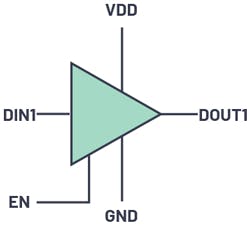
In this article, an LTspice model of a hypothetical ADxxxx device will be used to create an IBIS model. It’s a single-input and single-output digital buffer with an enable pin. Thus, the resulting IBIS model will have two inputs (DIN1 and EN) and a three-state output (DOUT1).
As a general guideline, there are five basic steps in generating an IBIS model:
- Set up the premodeling procedure.
- Perform LTspice simulations for C_comp, V-I, and V-T data extraction from the Spice model.
- Format the IBIS file.
- Check the file using the IBIS parser test.
- Compare the simulation results of IBIS model from the Spice model results under the same loading conditions.
The IBIS model provides the typical, minimum, and maximum data. They’re determined through the operating supply voltage ranges, temperature, and process corners. For brevity, only the typical conditions will be covered in this article.
The ibischk series of Golden Parser is useful to check the IBIS models to comply with the IBIS specifications. The ibischk executable file is available free of charge at IBIS.org. For this article, a third-party IBIS model editing software with integrated ibischk was utilized.
Premodeling Procedure
Before starting with the simulation, the user should have the device’s datasheet downloaded, as well as the Spice model and LTspice file installed. Perform initial evaluation of the part by determining the number of digital interfaces it has and what type it is (e.g., input, open-drain, 3-state, etc.).
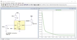
From the device datasheet, determine the operating supply voltage, operating temperature, integrated-circuit (IC) package type, device pinouts, loading conditions for timing specifications (RLoad and/or CLoad) for digital outputs, and the low-level input voltage (VINL) and high-level input voltage (VINH) for digital inputs. Figure 2 illustrates the ADxxx Spice model, and Table 2 lists its specifications.

All of the information regarding the digital interfaces of a device are put together in an IBIS file through the use of keywords. A keyword is an identifier in an IBIS model that’s enclosed by brackets, as discussed in Part 1 (please refer to it for more details).
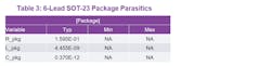
The keyword related to the IC package model is [Package]. It contains the RLC (resistance-inductance-capacitance) parasitics that represent the bonding from the die pad to the IC pad/pin. This information can be obtained from the manufacturer. One also can look for another IBIS file’s [Package] data if that device has the exact same package as the device being evaluated and comes from the same manufacturer. The device package parasitics for a 6-lead SOT-23 package is listed in Table 3.
The device pinouts are listed in Table 4. The keyword [Pin] is used to describe the pins and their corresponding model name. [Pin] is generally in a 3-column format. The first column is for the pin number, the second is the pin description, and the third is for the model name. Some packages have more similar pins (VCC, GND). These pins can be grouped and described together by the model.

In this case, given that a Spice model was given with no information about the internal transistor-level schematic, it’s good practice to have a separate model for each digital interface. Model names “Power” and “GND” are used to name power and ground pins in the IBIS file. Nondigital interfaces and “Do not connect” pins are described as “NC” or no connect. Take note that the model name is case sensitive. As they will be used later in the modeling procedure, the exact model name should be indicated.
Table 5 presents an ADxxxx truth table. This is useful when setting up an LTspice simulation. It’s important to know how to set the DOUT1 pin in high-impedance (high-Z) mode, Logic 1, and Logic 0.

LTspice Setup and Simulation
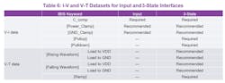
Generally, an IBIS model describes the behavior of digital buffers through I-V (current vs. voltage) and V-T (voltage vs. time) data as mentioned earlier. Each type of digital interface has its own set of I-V and/or V-T data needed in IBIS modeling as summarized in Table 1.
Those datasets are more elaborately presented in Table 6. Take note on the remarks for each dataset. Those tagged as “Recommended” mean that their absence will not result in an error in the ibischk parser test. However, these datasets have certain effects in channel simulation. For example, clamp data helps in analyzing signal reflections.
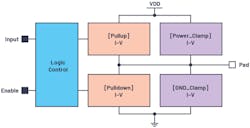
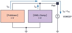
[Power_Clamp] and [GND_Clamp]
[GND_Clamp] and [Power_Clamp] show the behavior of the electrostatic-discharge (ESD) devices of the digital buffer through tabulated I-V data (Fig. 3). [Power_Clamp] represents the overall behavior of ESD devices referenced to VDD, while the ground clamp shows the overall behavior of the ESD devices referenced to GND.
![3. Conceptual diagram of [Power_Clamp] and [GND_Clamp] keyword structure.](https://img.electronicdesign.com/files/base/ebm/electronicdesign/image/2022/11/376626_fig_03.637b958ce430d.png?auto=format,compress&fit=max&q=45?w=250&width=250)
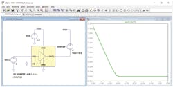
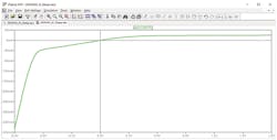
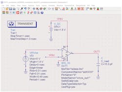
In LTspice, I-V data can be measured using the .DC Spice command/directive. The ground clamp of DOUT1 is measured using the setup in Figure 4. In the setup, appropriate supply voltages were applied to configure the device in a high-impedance state (refer to Table 5). This ensures that the ESD devices are isolated from the core circuit. VSWEEP is the sweep voltage referenced to GND. Referencing VSWEEP to ground ensures that only the GND clamp ESD device is characterized.
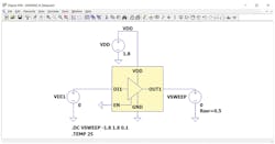
As per the IBIS specification, I-V data should be swept beyond the rail (preferably from –VDD to 2 × VDD)—in this case, from –1.8 V to +3.6 V. By doing this directly, sweeping voltage beyond VDD will turn on the power-clamp ESD device. To avoid this, initially sweep VSWEEP from –1.8 V to +1.8 V and use extrapolation methods to add that 3.6-V data point. This method is applicable for all I-V datasets.
In addition, note that all I-V datasets accept only up to 100 data points. Exceeding this number of data points will prompt an error on the ibischk parser test. Set the increment of the .DC command so that the resulting number of data points is less than or equal to 99. This is to accommodate that extra one data point for 2 × VDD extrapolation.
With dc sweeps, one might encounter very high reverse currents in simulations. To deal with this, set the start sweep from the approximate diode barrier potential (–0.7 V) to VDD (+1.8 V). Then extrapolate the data to comply with –VDD to 2 × VDD I-V data. Another way is to place a small resistor (Rser) in series with VSWEEP to limit the extreme currents.
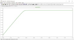
By clicking the Run button, LTspice runs the simulation. Since the DOUT1 is being evaluated, the node of interest is Ix(U1:DOUT1). Although the I(VSWEEP) also is technically correct, the polarity of the current on Ix(U1:DOUT1) is what’s needed on the IBIS model. This is to minimize further data formatting on I(VSWEEP) data to make it suitable for the model. The result should look like the graph in Figure 5.
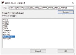
After simulation, save the data by clicking the Results window first, then click File -> Export data as text. Navigate on to the directory where you want to save, then click on the node under test, and then click OK (Fig. 6).
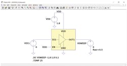
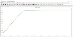
[Power_Clamp] data extraction is similar to the ground clamp setup, such that the sweep voltage (VSWEEP) is referenced to VDD. The setup and result are shown in Figure 7.
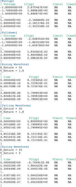
[Pulldown] and [Pullup]
Figure 8 shows the conceptual diagram of the I-V keyword structure. [Pulldown] and [Pullup] represent the behaviors of pullup and pulldown elements in a buffer. In graphical form, they look like the I-V characteristic curve of a MOSFET.
In extracting the data for [Pulldown] and [Pullup], it’s important to know how to manipulate the signal coming out of the output pin through the device’s truth table. The setup in extracting [Pulldown] and [Pullup] data is similar to [GND_Clamp] and [Power_Clamp]; it’s just that the DOUT1 pin is enabled and not in high-Z mode.
To extract data for [Pulldown], the DOUT1 pin should be set to Logic 0 output or 0 V. Thus, appropriate supply voltages must be put in place as depicted in Figure 9. Logic high voltage equivalent to 1.8 V was applied to the EN pin to enable the DOUT1 pin, and Logic 0 or 0 V was applied to the DIN1 pin to set the DOUT1 pin to Logic 0 output. This can be confirmed through the truth table presented in Table 5. The results are plotted in Figure 10.
Zooming in on the [Pulldown] data, it resembles the I-V characteristic curve of a MOSFET (Fig. 11).
In saving the pulldown data, take note that it constitutes to the total current from [GND_Clamp] and [Pulldown]. This can be better explained in the diagram from Figure 12. To remove the [GND_Clamp] component, simply subtract it from the [Pulldown] saved data point by point. To do this more easily, it’s important that the voltage increment, start voltage, and end voltage of the dc analysis of [GND_Clamp] and [Pulldown] be the same.
The setup in getting the pullup data is shown in Figure 13. Appropriate supply voltages were placed to set DOUT1 to Logic 1 (1.8 V). This ensures that the pullup elements are active/turned on. Then VSWEEP also is swept from –1.8 V to +1.8 V and referenced to VDD. Connecting VSWEEP this way prevents the user from formatting the data to conform to the IBIS specification.
Just like [Pulldown], the saved [Pullup] data is a result from the total [Power_ Clamp] and [Pullup] currents (Fig. 14). Therefore, users need to remove the [Power_Clamp] component by subtracting it point by point from the saved [Pullup] data. This can be done easily if their dc sweep parameters are the same. As a general reminder, use the same dc sweep parameters for all I-V data measurements.
![14. Actual current from [Pullup] saved data.](https://img.electronicdesign.com/files/base/ebm/electronicdesign/image/2022/11/376626_fig_14.637b971a1d0a9.png?auto=format,compress&fit=max&q=45?w=250&width=250)
[C_comp]
The [C_comp] keyword represents the buffer’s capacitance; it has different values for minimum, typical, and maximum corners. It’s the capacitance of the transistors and die and differs from the package capacitance. [C_comp] can be extracted in two ways: It can either be approximated using the formula in Equation 1, or be computed using the formula in Equation 2 when the pin is supplied by an ac voltage.


where ImIac is the imaginary value of the measured current, F is the frequency of the ac source, and VAC is the amplitude of the ac source.
C_Comp Extraction Using LTspice
The buffer capacitance could be extracted by supplying an ac voltage with a frequency sweep as shown in Figure 15. Since ac voltage is supplied, there will be real and imaginary parts of the current to be measured. The polarity of the current must be inverted to measure the value of the current flowing into the buffer while sourcing it with ac voltage. When measuring the output buffer capacitance, the only change that must be made from Figure 15 is that the ac source must be connected in the output pin.
An ac voltage will be supplied with any value of amplitude, but usually it’s set to 1 V. It will be processed by a frequency sweep as dictated in the Spice directives. When plotting the waveform using the .AC command, it’s set by default to display in Bode mode, which uses dB units. It must be set to Cartesian mode to see the numerical value of the current sothat it can be directly processed to the formula for the buffer capacitance.
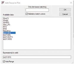
To view the waveform of the buffer capacitance, the user must first right click the Waveform window and click Add Trace, then select the pin being measured (Fig. 16). The waveform plot window will display two lines.
The solid line represents the real value of the measured current, while the dotted line represents the imaginary value of the measured current.
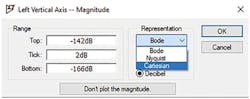
To change the plot settings from Bode to Cartesian, right click the y-axis on the left side of the waveform window and it should open the Left Vertical Axis—Magnitude dialog box. Then change the plot representation from Bode to Cartesian (Fig. 17).
LTspice Directives for C_Comp Setup
LTspice directives are used to set a circuit’s mode of operation, measure variables, and process parameters to compute for the C_comp. Listed below are the LTspice directives used to measure the buffer’s C_comp value:
- AC Lin 10 1k 10k: Sets the mode of operation of the circuit to AC linear frequency sweep from 1 kHz to 10 kHz.
- .Options meascplxfmt: Changes the default results of the .meas command to Bode, Nyquist, or Cartesian mode.
- .Options measdgt: Sets the number of significant figures for the .meas statement.
- .meas statements: These directives are used to find the value of certain parameters in the circuit.
These Spice directives can be modified depending on what parameter the user wants to display. A detailed explanation about the directives that are usable in LTspice can be found in “LTspice Help.” The result of the measure statements is viewable in Tools > SPICE Error Log (Fig. 18).
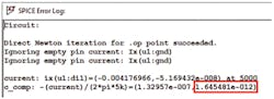
The results shown in the SPICE Error Log will be in Cartesian form. The x-coordinate is the real part of the current and buffer capacitance, while the y-coordinate shows the imaginary part of the current and buffer capacitance. As mentioned above, when measuring the buffer capacitance, the imaginary part of the current is needed for the buffer capacitance, so the actual value of the C_comp is the one highlighted in Figure 18.
What Are Rising and Falling Waveforms?
The [Rising Waveform] and [Falling Waveform] keywords model the switching behavior of the output buffer. Four V-T datasets are recommended for inclusion for an output model: rising and falling waveforms with a load referenced to ground and rising and falling waveforms with a load referenced to VDD.
Extracting the Rising and Falling V-T data
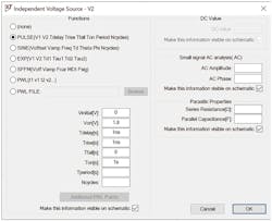
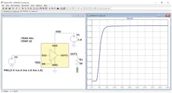
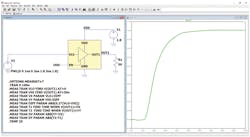
To extract the rising or falling waveforms of OUT1 in LTspice, a rising-edge or falling-edge input stimulus in the form of a piecewise linear (PWL) signal or pulse voltage supply is sent to the input pin (Fig. 19). The transition of the input stimulus used in the simulation needs to be fast to extract the fastest output transitions for the model.
Transient analysis will be performed on the schematic using the .TRAN command while measuring the voltage at the output pin. A 50-Ω resistor is used as the load for extracting the data of the four V-T waveforms for 3-state output buffers, but it may vary depending on the buffer design and drive capability to make an output transition. 50 Ω is the default load value for V-T data extraction because it’s the typical value of PCB trace impedance. The 50-Ω load is connected to the buffer’s output pin with respect to ground (load to ground) or VDD (load to VDD).
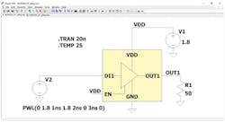
Falling Waveform with a Ground-Referenced 50-Ω Load
To produce a ground-referenced falling output waveform, a falling-edge input is needed and the 50-Ω load needs to be referenced to GND (Fig. 20). The resulting V-T waveform is shown in Figure 21, wherein the output settles at around 16 to 20 ns. It’s important to note that the transient analysis time should be enough to capture the falling waveform as it settles.
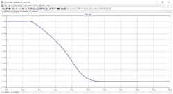
Falling Waveform with a VDD-Referenced 50-Ω Load
Figure 22 shows the setup and result for a falling waveform with a VDD-referenced 50-Ω load. As seen in the figure, the transient time needed is 50 ns to fully capture the falling transition of the output.
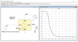
Rising Waveform with a Ground-Referenced 50-Ω Load
For the rising waveforms, a rising-edge input stimulus in the form of a PWL signal was used. In Figure 23, the setup shows a load resistance connected to the output pin with respect to ground, which will yield the V-T data for rising load to ground.
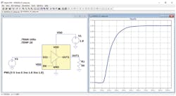
Rising Waveform with Load Connected to VDD
The same rising-edge input stimulus was used, but the 50 Ω needs to be referenced to VDD (Fig. 24).
One way of checking the correctness of the V-T data is by looking at the logic-low and logic-high voltages. VDD-referenced waveforms should have the same logic-low and logic-high voltage levels, and the logic-high voltage should be the same as VDD. On the other hand, GND-referenced waveforms also should have the same logic-low and logic-high voltages and the logic-low voltage level should be approximately 0 V.
Exporting the Waveform
The V-T waveforms extracted from the four setups must then be saved by performing the following steps (Figs. 25 and 26):
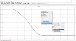
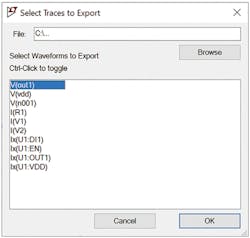
- Right-click on the Plot.
- Hover to File and click on Export data as text.
- Choose the waveform that will be exported and the directory where it will be exported.
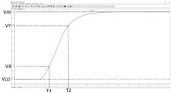
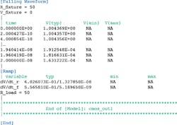
- VX and VY: represent the voltage at 20% and 80% point of the rising/falling transition edge.
- dV and dT: these are the computed values for the [Ramp] keyword for the IBIS model.
Ramp Data Extraction Using LTspice
The [Ramp] keyword is the ramp rate (dV/dt) representation of the rising and falling V-T data taken at 20% to 80% of the rising or falling transition edge. This method can be achieved on LTspice because it has the capability to compute those parameters using the .MEAS and .PARAM directives. The ramp extraction process can be done by adding Spice directives on the VT waveform setup. This implies that the ramp and VT waveform can be extracted at the same time.
Figure 27 shows the setup for the rising waveform’s ramp computation. For the falling waveform’s ramp computation, the time values for VLO and VHI should be interchanged since the output waveform for the falling ramp starts at the buffer’s logic high and transitions into logic low.
LTspice Directives for Ramp Extraction
The Spice directives used for ramp extraction are: .TRAN, which is the Spice directive used for the VT rising/falling waveform; .OPTIONS, to set the output that will be displayed on the Spice Error Log to Cartesian mode and limit it to the desired number of significant digits; and .MEAS, for the actual computation of the ramp (Figs. 27 and 28):
- VLO: Represents logic low voltage.
- VHI: Represents logic high voltage.
- Diff: Represents the voltage at the 20% point of the transition where this will be added and subtracted to the VLO and VHI parameters, respectively, to get the 20% and 80% point of the transition.
Building the IBIS Model
All extracted I-V and V-T data are compiled to the IBIS model (.ibs) file. Below is an actual template of the IBIS file, which the user can use as a reference in building the IBIS model (see IBIS file 1).
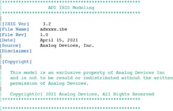
An .ibs file starts with the [IBIS Ver] keyword, followed by its file name and revision number. IBIS version 3.2 will be used in the [IBIS Ver] keyword since it’s the minimum version needed to model a 3-state output buffer. The file name of the .ibs file and the file name in the [File Name] keyword should be the same; otherwise, the parser will detect it as an error. In addition, the file name should not contain any uppercase letters because the parser only allows lowercase letters to be used in the file name. Other important keywords will be discussed in the latter part of this section.
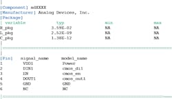
The next part of the .ibs file includes the [Component], [Manufacturer], [Package], and [Pin] keywords (see IBIS file 2). ADxxxx has two input buffers (DIN1 and EN) and one output buffer (DOUT1), so its IBIS model will have a total of three buffer models. The [Package] keyword serves as the package model of the device through RLC package parasitic values. The model names for all device buffers are defined under the [Pin] keyword, which is similar to the naming variables and defined under the [Model] keyword.
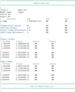
In the next part of the .ibs file, the device’s digital buffers are modeled using the measured I-V and V-T data (see IBIS file 3). The contents of a buffer model vary depending on the buffer type specified in the Model_type variable. Since the model cmos_di1 is an input buffer, its buffer model only includes C_comp, [Power_Clamp], and [GND_Clamp] data. An input buffer model also contains its VINH and VINL values, which can both be found in the device datasheet. Given that DIN1 and EN are both input buffers, their buffer model has the same structure.
A 3-state buffer model, on the other hand, contains some keywords similar to an input buffer model but with additional I-V and V-T data. The buffer model of cmos_out1 includes additional sub-parameters—Cref, which represents the output capacitive load, and Vmeas, which represents the reference voltage level (see IBIS file 4). Usually, the Vmeas being used is half the value of VDD.
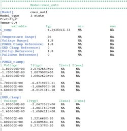
Aside from C_comp, [Power_Clamp], and [GND_Clamp], a three-state buffer has additional I-V data: [Pullup] and [Pulldown] (see IBIS file 5).
Lastly, all IBIS models should be closed with the [End] keyword (see IBIS file 6).
IBIS Model Validation
As discussed in Part 1, the IBIS model validation is comprised of a parser test and correlation process. These are necessary steps to ensure that the IBIS file complies to the IBIS specification and the model performs as close as possible to the reference Spice model.
Parser Test
The IBIS file created in the previous section should first undergo a parser test before moving forward to the correlation process. The ibischk is the Golden Parser used to check the IBIS file. This checks the compliance of the IBIS file to the specification set by the IBIS association. More details are available at ibis.org. At the time of writing this article, the latest parser being used is ibischk version 7.
In performing a parser test, it’s best to use IBIS model editing software with integrated ibischk, such as Cadence Model Integrity and Hyperlynx Visual IBIS Editor. These tools provide ease in checking the syntax. However, if the user doesn’t have any of these, the executable code is free of charge at ibis.org. It’s compiled at a variety of operating systems, so users needn’t worry about which operating system to use.
Correlation Procedure
In this stage of validation, the IBIS model needs to be checked if it performs like the reference, which, in this case, is the Spice model. Table 7 shows the different IBIS quality levels from Level 0 to Level 3. It describes how accurate the IBIS model is to the reference, depending on the test it has undergone.

In this case, since the reference is an ADxxxx Spice model, the generated IBIS model can qualify for Level 2a. This means that it passes the parser test, it has a correct and complete set of parameters as described in the datasheet, and it passes the correlation procedure.
To correlate the IBIS model to the reference Spice model, there are general steps that can be followed. These are summarized in the flow diagram shown in Figure 30.
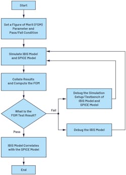
Setting the Figure of Merit
The basis of correlation is that the IBIS model should behave the same as the Spice model digital interface under the same loading conditions and input stimuli. This means that their outputs should theoretically lie directly on top of each other. In general, there are two ways to describe how close the IBIS model output is to the Spice model reference: qualitative and quantitative. Users can employ these two means to determine how the IBIS model correlates to the Spice model.
A qualitative figure-of-merit (FOM) test utilizes the user’s observations. It involves visual inspection of the two outputs to determine whether the correlation passes. This could be done by superimposing the output results from both IBIS and Spice and use engineering judgment to determine whether the graphs correlate or not. It can serve as a preliminary test of correlation before it proceeds to the quantitative FOM test. This test is sufficient when the interface operates at a relatively low frequency or bit rate.
Another qualitative FOM test was presented in the IBIS IO Buffer Accuracy Handbook, which is the curve envelope metric. It uses the minimum and maximum curves defined by the process voltage temperature extremes. The minimum and maximum curves serve as a boundary for correlation. To achieve a pass mark, all of the points on the IBIS results should fall within the minimum and maximum curves. This method isn’t applicable in this article because it’s limited to typical conditions only.
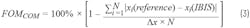
A quantitative FOM test uses mathematical operations to measure how IBIS correlates with Spice. The curve overlay metric, which also was presented in the IBIS IO Buffer Accuracy Handbook, uses the data points of IBIS and Spice outputs. It computes the summation of the absolute value of the x-axis or y-axis differences between the IBIS and reference data points divided by the product of the total range used in the axis and the number of points. This is illustrated in Equation 3 and is suitable as a correlation method in the use case presented in this article.
However, other factors still should be considered. The FOM presented in Equation 3 has a requirement that the results from both IBIS and Spice should be mapped on a common x-y grid, and this will use numerical algorithms and interpolation methods. If the user wants to do a quick quantitative FOM test, this article presents another method, the curve area metric, which uses the area bounded by the curve and x-axis.
The curve area metric compares the computed area under the curve of IBIS using the Spice result as the reference. It’s defined in Equation 4. However, it’s required that the created model passes the qualitative test before proceeding to the curve area metric test. This ensures that the IBIS and Spice curves are in-phase and laid on top of one another.
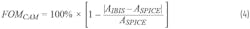
In getting the area under the curve, the user can use numerical methods such as the trapezoidal rule or midpoint rule, given the same method is used on both the IBIS and Spice results. When using this method, it’s recommended to have as many points as possible to better approximate the area.
Validating the ADxxxx IBIS Model
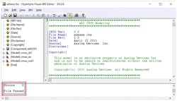
As mentioned, the first step of IBIS model validation is the parser test. Figure 31 shows the parser test results of an adxxxx.ibs IBIS model file, which was written using the HyperLynx Visual IBIS Editor. When the user performs the parser test, the goal is to receive no errors. If there are any error or warning prompts, the model maker needs to fix them. This guarantees compatibility of the IBIS model among simulation tools.
The next step involves setting up the FOM parameter. This article is limited to the use of the qualitative FOM and curve area metric as measures of correlation. The test will involve the transient response curves from IBIS and Spice using the same loading conditions and input stimuli. The calculated curve area metric FOM should be ≥95% to pass the correlation. The DOUT1, DIN1, and EN correlations are described below.
DOUT1
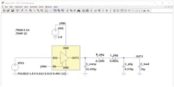
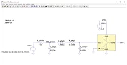
The Spice testbench on LTspice for DOUT1 correlation is shown in Figure 32. Appropriate voltage supplies were placed on the schematic to enable the driver; a pulse signal source is placed on the DIN1 pin to drive DOUT1. Additional components are needed to complete the DOUT1 driver model in LTspice. The C_comp represents the die capacitance. After adding C_comp and C_load to the LTspice model, the RLC package parasitics (R_pkg, L_pkg, C_pkg) and C_load are placed.
The DOUT1 IBIS model correlation testbench was set up on the Keysight Advanced Design System (ADS) (Fig. 33). The same input stimuli, C_load, voltage source, and transient analysis were used as the LTspice testbench. However, the C_comp and RLC package parasitics weren’t placed on the ADS schematic because they were already included on the 3-state IBIS block.
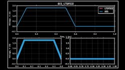
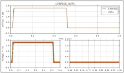
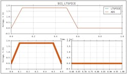
The transient response curves are measured from the C_load. LTspice and ADS results have been compared and laid on top of one another for qualitative FOM. As seen in Figure 34, the LTspice and ADS DOUT1 responses are very similar. The difference can be quantified with a curve area metric. The area under the curve is computed for the duration of a 1-µs transient. The computed curve area metric is 99.79%, which satisfies the set ≥95% pass condition. Thus, the DOUT1 IBIS model correlates to the Spice model.
DIN1 and EN
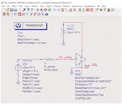
In validating the input port, the transient response curves from LTspice and ADS will be correlated through the qualitative FOM and curve area metric. The testbench in LTspice is shown in Figure 35. This is applicable for both the DIN1 and EN pins.
Like DOUT1, the extracted C_comp is placed right at the DIN1 port, then followed by the RLC package parasitics. After that, a 50-Ω R_series resistor followed by an input stimulus pulse voltage supply are connected. The probe point for measuring the response is at DIN1_probe.
Figure 36 shows the Keysight ADS testbench for validating input ports. Similarly, an R_series 50-Ω resistor is placed before the input port and the same input pulse stimulus is used. The C_comp and RLC parasitics aren’t placed because they’re already included in the IBIS block. The probe for the measurement of transient response is at DI1_probe.
The transient response curves from LTspice and ADS were laid on top of one another for the qualitative FOM test. As seen in Figure 37, the curves are the same—the LTspice curve is completely behind the ADS curve. The computed curve area metric for DI1 is at 100%, which satisfied the set ≥95% pass condition. The same plot and curve area metric also were obtained from EN pin correlation results.
Final Thoughts
The article presented a methodology on how to extract data and build an IBIS model using LTspice. It also described a way to correlate the IBIS model to the reference Spice model through qualitative FOM and quantitative FOM through the curve area metric. For users, this could bring a level of confidence that the IBIS model behaves similarly to the Spice model.
Although other types of digital IO aren’t presented here, the procedure in extracting C_comp, I-V data, and V-T data may serve as a stepping-stone in creating other types of IO models. You can download and install LTspice for free and start creating your own IBIS models.
Read more articles in the Test & Measurement library series: Simulate Your Way to Design Success with IBIS Modeling.
References
Casamayor, Mercedes. “AN-715 Application Note: A First Approach to IBIS Models: What They Are and How They Are Generated.” Analog Devices Inc., 2004.
IBIS. I/O Buffer Accuracy Handbook. IBIS Open Forum, April 2000.
Leventhal, Roy and Green, Lynne. Semiconductor Modeling: For Simulating Signal, Power, and Electromagnetic Integrity. Springer, 2006.
Mirmak, Michael; Angulo, John; Dodd, Ian; Green, Lynne; Huq, Syed; Muranyi, Arpad Muranyi; and Ross, Bob. IBIS Modeling Cookbook for IBIS Version 4.0. The IBIS Open Forum, September 2005.
About the Author
Rolynd Troy Aquino
Product Applications Engineer, Analog Devices Inc.
Rolynd Troy Aquino is a product applications engineer at Analog Devices working under the New Technology Integration Team. His focus is on IBIS, IBIS-AMI, and LTspice modeling and simulations for ADI products. He became an ADI intern in 2014 and officially joined ADI in 2016. He graduated from Mapúa University in Manila with a Bachelor’s degree in electronics engineering in 2015.
Comment About the Article
To join the conversation, and become an exclusive member of Electronic Design, create an account today!

Leaders relevant to this article: