The World’s Smallest Development Electronics

What you’ll learn:
- Perovskite-based LED Pixels
- Cerebras Systems WSE-3 Chip
- Solidigm D5-P5336 SSD
- IBM Condor Quantum Chip
- Hugging Face DistilBERT LLM
- Northrop Grumman 1-THz Microchip
- Highest Wireless Data-Transmission Speed
- Highest Electron Microscope Resolution
- Single-Atom Transistor
- 1-nm Gate Transistor
From AI-powered processors to atomic-scale transistors, the world of microelectronics is continually being redefined by how small, how powerful, and how energy-efficient devices can become. Whether it's packing record-breaking pixel densities into virus-sized LEDs or cramming trillions of transistors into a single wafer, today’s innovations are pushing the limits of Moore’s Law and manufacturing.
In this roundup, we take a look at some of the most impressive “world firsts” in small-scale electronics that are shaping the future of computing, storage, sensing, and display technologies.
Perovskite-based LED Pixels
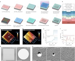
Researchers from Zhejiang University and the University of Cambridge have developed LED pixels utilizing perovskite semiconductors. The pixels are as small as 90 nm, about the size of a virus, and pack a record pixel density of 127,000 pixels per inch. According to the researchers, the pixels retain their brightness and efficiency at that level, providing a cost-effective alternative to traditional LEDs.
While the current prototypes only provide monochrome light, further development is needed to produce full RGB displays. The advance could lead to ultra-high-resolution displays for mobile devices, TVs, and augmented-reality platforms.
Cerebras Systems WSE-3 Chip
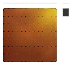
The WSE-3 (Wafer Scale Engine) chip developed by Cerebras Systems currently holds the title of the world’s fastest wafer-scale AI chip, which integrates a large number of cores and transistors into a single, albeit large, chip. The AI chip packs 4 trillion transistors, 900,000 AI cores, and 44-GB on-chip SRAM, and it can handle up to 1.2 PB of external RAM.
The chip, manufactured using the 5-nm TSMC process, provides up to 125 PFLOPS of peak AI performance and can train AI models up to 24 trillion parameters. The monstrous chip forms the basis of Cerebras’s CS-3 computer, which is about the size of a mini-fridge and optimized for AI workloads.
Solidigm D5-P5336 SSD

Solidigm’s D5-P5336 is a high-capacity, enterprise-grade solid-state disk (SSD) designed for workloads in data centers and AI applications. It was the world’s first SSD to offer a storage capacity of 122.88 TB, making it one of the highest-capacity SSDs available, comparable only to DapuStor’s 122.88-TB SSD, which was announced shortly after Solidigm’s release.
The D5-P5336 provides sequential read speeds up to 7,000 MB/s and write speeds up to 3,300 MB/s, utilizes the PCIe 4.0 x4 with NVMe protocol, and is rated for 5,900 TBW (terabytes written). According to Solidigm, the drive is part of its fourth-generation QLC (quad-level cell) SSDs and stores four bits per cell, allowing for higher storage density compared to TLC (triple-level cell) SSDs.
IBM Condor Quantum Chip
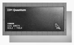
Unveiled in 2023 by IBM, the Condor quantum processor boasts a whopping 1,121 qubits and remains the world’s fastest qubit-based processor. The processor takes advantage of IBM’s cross-resonance gate technology—a two-qubit gate mechanism that enables entanglement between fixed-frequency transmon qubits without necessitating tunable couplers.
The Condor provides a 50% increase in qubit density compared to its predecessor, Osprey, enhancing computational capabilities within a similar footprint. What’s more, the processor incorporates over a mile of high-density cryogenic flex I/O wiring within a single dilution refrigerator, leading to efficient communication between qubits. The processor, currently packed into IBM’s Quantum System Two, is designed for scalability and allows for even larger quantum processors coming down the pipeline.
Hugging Face DistilBERT LLM

Touted as an efficient and compact version of BERT (Bidirectional Encoder Representations from Transformers), Hugging Face’sDistilBERT is the world’s smallest practical large language model (LLM). It retains most of its performance while reducing its size and computational requirements. DistilBERT was trained using the knowledge distillation method, where a smaller model, known as a “student,” is trained to mimic the behavior of a larger pre-trained model, known as a “teacher.”
During the training process, the student learns to produce the logits (output values from the last layer of a neural network that hasn’t been normalized into probabilities), embeddings, and attention maps derived from the teacher. Due to its smaller size, DistilBERT is ideal for use with real-time applications, including chatbots, natural language processing, named entity recognition, and more.
Northrop Grumman 1-THz Microchip

Northrop Grumman debuted its 1-THz microchip back in 2014, and eventually was entered into The Guinness Book of World Records for the fastest integrated-circuit amplifier ever created. The chip operates at 150 billion cycles faster than the previous record of 850 GHz, set in 2012, according to Northrop, which built the device with funding from DARPA (Defense Advanced Research Projects Agency).
Terahertz is a block of the electromagnetic spectrum that’s situated between microwaves and infrared light waves. Researchers have been trying to exploit this high-frequency band, traditionally known as the "terahertz gap," but have been unable to detect, process, and radiate the necessary high-frequency signals without resorting to frequency translation or multiplication.
The terahertz monolithic integrated circuit (TMIC) bridges that gap by utilizing a super-scaled 25-nm gate length, indium-phosphide, high electron mobility transistor that measures at a gain of 10 dB at 1 THz and 9 dB at 1.03 THz. To put that into perspective, current smartphones operate at 1 to 2 GHz and wireless networks at 5.7 GHz.
Highest Wireless Data-Transmission Speed
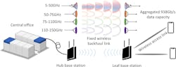
In 2024, engineers from UCL achieved a world record for the fastest wireless data transmission by achieving a blistering 938 Gb/s. According to UCL, this was accomplished by utilizing an ultra-wide 145-GHz bandwidth wireless transmission of orthogonal frequency-division multiplexing (OFDM) signals over the air, which covers the 5- to 150-GHz frequency spectrum.
The engineers achieved that speed by combining high-speed electronics and microwave photonics technologies. The signals, over 5 to 75 GHz, are generated using high-speed digital-to-analog converters (DACs). The high-frequency millimeter-wave (mmWave) band signals, including W-band (75 to 110 GHz) and D-band (110 to 150 GHz) signals, are generated by mixing optically modulated signals with frequency-locked lasers on high-speed photodiodes.
The engineers then frequency-locked two pairs of narrow linewidth lasers, referred them to a common quartz oscillator, and generated W-band and D-band signals with stable carrier frequency and reduced phase noise. By using the OFDM format and bit loading, they produced a 938-Gb/s transmission data rate with less than a 300-MHz gap between different RF and mmWave bands.
Highest Electron Microscope Resolution
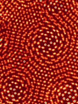
Engineers from Cornell University gained the crown for the world’s highest electron microscope resolution, measuring down to 0.39 angstroms (0.039 nm), allowing for imaging at the atomic scale. To accomplish that feat, the engineers employed their electron microscope pixel array detector (EMPAD), which was developed back in 2017.
Cornell’s EMPAD is equipped with a 128 × 128 array of electron-sensitive pixels, each 150 µm (millionths of a meter) square, which is bonded to an integrated circuit that reads out the signals. It doesn’t produce an image in the traditional sense, like the array of light-sensitive pixels in the sensor of a digital camera. Instead, it detects the angles at which electrons emerge as each electron hits a different pixel. The engineers then used a technique known as ptychography to produce an image that’s reconstructed from the microscope’s 4-dimensional dataset.
Single-Atom Transistor

Scientists from Germany’s Karlsruhe Institute of Technology (KIT) developed the world’s smallest quasi-solid-state transistor, which operates via the switching action of a single atom. The single-atom transistor operates at room temperature and consumes very little energy, suiting it for use in next-gen technologies.
The scientists designed their single-atom transistor using a pair of tiny metal contacts with a gap that’s the width of a single metal atom between them. An electrically controlled pulse pushes a single silver atom into the gap, which closes the circuit. Pushing that atom back out breaks the circuit. Since the transistor is created entirely of metal and uses a solid electrolyte, there’s no need for semiconductor materials or large amounts of power to function.
1-nm Gate Transistor
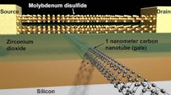
The engineers created their 1-nm-gate transistor using molybdenum disulfide (MoS2), commonly known as engine lube, and carbon nanotubes. MoS2 is part of a family of materials with massive potential for applications in LEDs, lasers, solar cells, and more.
According to the engineers, conventional lithography techniques don’t work well at such small scales, so the researchers utilized carbon nanotubes. They then measured the electrical properties of the devices to show that the MoS2 transistor with the carbon-nanotube gate effectively controlled the flow of electrons. They have yet to develop a chip based on the technology, but it does lay the foundation to go beyond the 5-nm manufacturing process.
Conclusion
From quantum processors to one-atom transistors, these groundbreaking technologies represent more than just a world’s first. They're the foundation for the next generation of AI systems, ultra-high imaging, and tiny machines. As engineers, researchers and scientists continue to shrink hardware while boosting performance, the world is watching how the future of electronics unfolds one nanometer at a time.
About the Author

Cabe Atwell
Technology Editor, Electronic Design
Cabe is a Technology Editor for Electronic Design.
Engineer, Machinist, Cartoonist, Maker, Writer. A graduate Electrical Engineer actively plying his expertise in the industry and at his company, Gunhead. When not designing/building, he creates a steady torrent of projects and content in the media world. Many of his projects and articles are online at element14 & SolidSmack, industry-focused work at EETimes & EDN, and offbeat articles at Make Magazine. Currently, you can find him hosting webinars and contributing to Electronic Design and Machine Design.
Cabe is an electrical engineer, design consultant and author with 25 years’ experience. His most recent book is “Essential 555 IC: Design, Configure, and Create Clever Circuits”
Cabe writes the Engineering on Friday blog on Electronic Design.
See Cabe's cartoons & comic strips here.
Comment About the Article
To join the conversation, and become an exclusive member of Electronic Design, create an account today!

Leaders relevant to this article: