Members can download this article in PDF format.
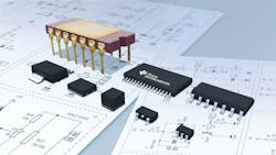
Today, advances in semiconductors and ICs are producing ever smaller and denser circuits. With that comes the challenge of efficiently packaging and interfacing these next-generation devices between the analog and digital worlds.
This is no simple task, considering the myriad requirements and specifications of electronics and products in today’s market. New circuits are being developed, and existing circuits are constantly evolving, which generally demands redesigning the repackage.
For example, new battery-management chips such as the BQ40Z50-R2 now combine low-cost logic, flash memory, and high-precision voltage measurement on a stacked die. This replaces the long-standing practice of separate circuits connected physically on the printed circuit board (PCB) and requires a package redesign.
The Importance of Package Design
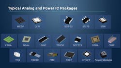
Today, the offering of package types is staggering (Fig. 1). There are dozens of unique designs, each customized for a particular electrical, mechanical, or thermal specification.
The convergence of analog and digital technologies within complex systems, spanning micro to macro, underscores the growing significance of package design. This integration often requires novel packaging designs that not only ensure the protection of the chip, but also the integrity of each signal, the effectiveness of power distribution, and the reliability of performance in real-world conditions.
Inside the Box
Gone are the days when the package was a simple metal or plastic case popped over the guts. Today’s packages are complex designs that interconnect the analog and other semiconductor parts to the PCB. A typical power package, for example, will have multiple features integrated into the package, saving space, time, and money.
For an example, let’s dissect TI’s MagPack series power modules (TPSM8286x). These modules offer excellent performance precisely because of the close integration with the magnetic package and analog components. This integration also increases power density and efficiency as well as reducing temperatures. On top of that, it minimizes board space and system power losses.
Packaging for the Future
Jockeying for board real estate has become a major factor in the design loop. The pressure to make systems smaller and cheaper has never been as demanding as it is today.
As advancing semiconductor technologies integrate with the digital world, dies will continue to shrink. Therefore, packages need to be more efficient — in all ways — yet provide the same or better performance, as well as lower cost and smaller footprints.
Take the high-power segment. Until recently, designs typically used discrete FETs and regulators with an external controller. The interconnect technology consisted of gold wire bonds to minimize electrical resistance. However, this technique proved expensive once gold started its meteoric rise (similar conditions occurred among other materials). So, designers were tasked with redesigning the package to be able to connect to copper wire bonds.
In that same vein, an edge-of-the-envelope process was to design vertical FETs (vFETs) with copper clip technology. Again, reducing footprint while maintaining or increasing power performance.
Similar advances have seen the integration of CMOS and bipolar designs on the same chip. This enabled the development of higher-performance FETs with integrated controllers.
However, to be able to use these devices, a low-resistance path was required between the package and the PCB. Designers addressed this by designing special, low-resistance copper bumps, which allowed for closer connections to the PCB’s power circuity.
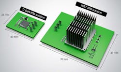
Similarly, GaN-based intelligent power modules (IPMs) (Fig. 2) have evolved from an insulated gate bipolar transistor (IGBT) IPM solution to a gallium-nitride (GaN)-based IPM. As can be seen in Figure 2, redesigned package technology resulted in the same 250-W performance with a 65% reduction in board real estate.
Driving Toward Miniaturization
The pressure to miniaturize devices while improving functionality, lowering costs, and reducing power is creating innovative packaging designs that were impossible only a few short years ago.
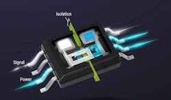
Today’s miniaturization techniques have enabled integrated devices that were previously difficult or impossible to develop. One example is isolation. This has always been a challenge with miniaturization because of the reduced proximity of interconnect wires. Wires too close to each other can create arcing paths and other interference issues.
One solution is to use magnetic isolation (Fig. 3). The goal is to solve inter-lead interference by means other than an air gap. As the packages get smaller, air-gap distances are no longer sufficient. Therefore, to enable both signal and power to exist within small packages, the packaging uses magnetic isolation to prevent signal or power corruption.
Integration: The Power Pill
The integration of analog and digital circuits within a single package has created a new level of opportunity. For instance, the integration of antennas within the package has opened the door for placement of extremely small form factor sensors in constrained locations such as automotive door handles.
On the higher power side of power, for the automotive sector, the newest automotive-qualified GaN device for powering onboard charging systems in electric vehicles incorporates a FET and a rapid-switching silicon gate driver. This module offers automotive designers a simplified, cost- and time-saving method of integrating a switch, controller, and protection technologies onto a thermally enhanced, single chip package.
Conclusion
This article offers a peek into some of what the packaging segment is coming up with and the challenges they face. The package is now taking its rightful place in the design chain. And not just as a placeholder, but as a device that enhances performance, reduces cost and board space, and is tightly coupled with circuit and device performance.