This file type includes high resolution graphics and schematics when applicable.
Analog-to-digital converters (ADCs) are used in a wide range of applications, particularly measurement systems that need to process analog transducer signals. Examples include data-acquisition systems to measure pressure, flow, velocity, and temperature. Typically, these signals are time-domain signatures in the form of a pulse or step function.
In any design, it’s important to understand the overall system accuracy, especially when systems must quantify very small sensitivities or changes in a waveform. In an ideal case, for every 1 V applied to the input of a signal chain, a 1-V output is digitally represented by the ADC. However, this is not the case. All converters, and all signal chains for that matter, have some finite amount of error associated with them.
Of particular interest are the errors associated with the ADC itself. Multiple inaccuracies accumulate within the converter to cause these errors. Understanding how this happens can help clarify how best to specify an ADC when defining system parameters for a new design.
ADC Inaccuracy
In any signal chain, the converter is the foundation of the system. System accuracy can be no better than the converter’s least-significant-bit (LSB) size.
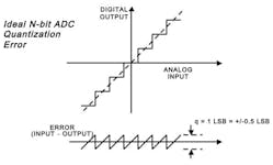
Because ADCs are not ideal and don’t exhibit infinite resolution, they can only output a finite number of representations. The actual number of representations is equal to the input full scale of the converter divided by 2N, with N being the nominal number of bits that the converter puts out per conversion (Fig. 1).
For example, for any voltage applied to its input, a 12-bit ADC may output one of 4096 unique digital representations to represent it. These representations have some finite amount of error. Therefore, if the 12-bit ADC’s datasheet specifies an input full-scale voltage (VFS) value of 10-VPP, its LSB would be 2.44 mVPP and, ideally, an accuracy of ±1.22 mV.
LSB = VFS/2N = 10/4096 = 2.44 mV = ±1.22 mV (1)
In reality though, ADCs are not ideal. Some finite amount of noise (k × T/C) exists within the converter itself—even at dc. Remember, a 1-kΩ resistor is equivalent to 4nV/√(Hz) in a 1-Hz bandwidth at 25°C. Notice that when looking at a 12-bit ADC datasheet, the signal-to-noise ratio (SNR) is typically on the order of 70 to 72 dB. However, a 12-bit ADC should have 74-dB SNR in the ideal world, based on:
SNR (dB) = 6.02 × N+1.76 (2)
Therefore, in the real world, 12-bit precision cannot be achieved, because the converter itself introduces inaccuracies (Fig 2).
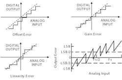
These inaccuracies or errors define how effective the converter represents the signal that ultimately is acquired throughout the signal chain. Such errors include:
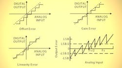
• Offset error: The analog value by which the transfer function fails to pass through zero.
• Gain error: The difference in FSV between the ideal and actual transfer function when offset error is zero.
• Linearity error (commonly referred to as nonlinearity): The deviation from a straight line drawn between zero and full scale as shown in Figure 1.
More ADC Inaccuracies
Now that the most basic ADC errors have been defined and understood, it’s useful to compare them. Typically, an ADC’s offset and gain errors are so small that they can be either ignored or adjusted (nulled) by means of an external analog circuit or via digital processing. However, other errors, such as linearity, quantization, and temperature coefficient (“tempco”), cannot be so easily adjusted or eliminated.
ADC linearity is only as good as the converter itself, which means it’s influenced by architecture and process variation. To deal with nonlinearity, the designer generally has two choices: either purchase a better—and more expensive—converter, or digitally correct the linearity.
Digital correction can turn out to be as costly as buying a better converter, though, because it demands more resources on the DSP or FPGA, as nonlinearity will shift over temperature and process variation. Depending on the sample rate, IF, and resolution, digital correction may require extensive characterization and look-up tables to correct or adjust the ADC’s performance on the fly.
DNL and INL
Linearity involves two types of errors—differential and integral linearity (DNL and INL, respectively). DNL is defined as any error or deviation from the conversion’s ideal value. In other words, it’s the deviation in the analog difference between two adjacent codes from the ideal code value of VFS/2N.
Think about this in relation to SNR performance of the ADC. As the code variation grows, the number of transitions shrinks. This error is bound to ±0.5 LSBs over temperature to ensure no missing codes.
INL is defined as the curvature deviation from an ideal straight-line approximation of the transfer function between zero and full scale. INL, for the most part, determines the spurious-free dynamic range (SFDR) performance of the ADC.
The shape of the overall INL deviation affects harmonic performance. For example, a “bow” in the INL curve will yield worse even-order harmonics, and an “s-bow” in the INL curve will commonly yield odd-order harmonics. However, because this error is frequency-dependent, it doesn’t relate to the type of error analysis under consideration here.
Thus, even though a null in the static offset and gain errors is feasible, the temperature coefficient related to offsets and gain errors will still exist (for example, a 12-bit ADC with 10-ppm gain error; or FSR/°C = 0.001%/°C). Likewise, 1 LSB in a 12-bit system is equivalent to 1 part in 4096, or approximately 0.024%.
So, a 125°C delta (–40 to +85°C) yields a ±2.5-LSB gain temperature error, or 0.001% × 125 = 0.125%, in which 0.125/0.024 = 5.1 or ± 2.55 LSBs.
For offset tempco, a 5-ppm offset error or FSR/°C = 0.0005% per °C. This would yield a ±1.3-LSB offset temperature-coefficient error, or 0.0005% × 125 = 0.0625, in which 0.0625/0.024 = 2.6 or ±1.3 LSBs.
ADC Error Analysis
Other error sources that can also play a role in the converter’s performance are common-mode rejection ratio (CMRR), clock jitter, and inherent board noise and coupling. All of these errors ultimately determine how effective the ADC is at representing a signal and usually exhibit their effects more obviously in the frequency domain.
From a time-domain standpoint, the following five errors dictate the converter’s overall accuracy:
• Relative accuracy, or DNL, which was defined as ±0.5 LSBs
• Relative DNL is the typical number in the datasheet. Relative tempco DNL is the DNL variation over rate temperature of the ADC/device/IC.
• Gain tempco error, which was ±2.5 LSBs (from the example above)
• Offset tempco error, which was ±1.3 LSBs (also from the example above)
• Power -supply sensitivity, which is typically expressed in terms of low-frequency power-supply rejection ratio (PSRR) within the first Nyquist zone. This can be typically expressed as 60 dB or ±2 LSBs for a 12-bit ADC.
By simply taking the root-sum-square (RSS) of all these error sources, total converter error will equal ±3.5 LSBs, which might seem overly pessimistic. Yet a statistical tolerance may actually be overly optimistic, or in other words, the total sum of errors divided by the number of errors or (0.5 + 2.5 + 1.3 + 2)/4 = ±1.58 LSBs. The actual tolerance of the ADC should fall somewhere between these two, though.
Therefore, when adding accuracy errors in the converter, or in any accuracy system analysis, designers should use a weighted error source approach, then RSS these error sources together. This will provide the best method in determining the ADC’s overall error.
As a result, the relative accuracy of ±0.5 LSBs should stay at 100%. However, the gain temperature compensation error of ±2.5 LSBs should be 66% of the total error or 2.5/(0.5+1.3+2) × 100. The offset compensation error of ±1.3 LSBs would be 26% of the total error or 1.3/(0.5+2.5+2) × 100. The power supply sensitivity error of ±2 LSBs would be 47% of the total error, or 2/(0.5+1.3+2.5) × 100. Adding these weighted errors together in an RSS fashion, or √((0.5×1)2 + (2.5 × 0.66)2 + (1.3 × 0.26) 2 +(2 × 0.47) 2), provides a total error of ±2.0 LSBs, which yield something more realistic in between the optimistic and pessimistic methods outcomes given earlier.
Accuracy in ADC Bandwidth
The ADC has a settling-time inaccuracy, too. Keep in mind that a converter’s internal front end must have enough bandwidth (BW) to accurately sample the signal. Otherwise, an accumulation of errors will be greater than what was described above.
In general, an ADC’s internal front end must settle within half a period of the sample clock cycle (0.5/Fs, where Fs = sample frequency) to provide an in-bounds accurate representation of the analog signal to be acquired. Therefore, for a 12-bit ADC sampling at 2.5 Gsamples/s and a full-scale input range of 1.3 VPP, the full-power bandwidth (FPBW) required can be derived by starting with the transient equation:
1 LSB = VFS × e(-t/τ)
Solving for t:
t = – τ × ln(1 LSB/VFS)
Substituting in τ = 1/(2 × π × FPBW) for one time constant, and solving for FPBW:
FPBW = –(1/(2 × πt) × ln(1 LSB/VFS)
let t = 0.5/Fs. That is the time needed for a sample to settle, where the sampling period is 1/Fs:
FPBW = –(Fs/π × ln(1 LSB/VFS) = –(2.5 G/π) × ln(317 µVPP /1.3)) = 6.62 GHz
This will yield the minimum required bandwidth for the ADC’s internal front-end FPBW. The converter’s internal front end needs this amount of BW to settle within 1 LSB and sample the analog signal appropriately. It will require the passage of several time constants to meet an accuracy of 1 LSB for this type of ADC, where one time constant is equal to 24 ps, or:
τ =1/(2 × π × FPBW)
To understand the number of time constants required for the full-scale range of the ADC in LSB size, %Full-scale error, or %FS, needs to be found. Or, 1 LSB = FS/(2N), where N = number of bits; or 1.3 VPP/(212) = 317 μVPP, and %FS = (LSB/FS) ×100 = 0.0244.
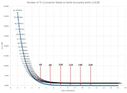
By plotting Euler’s number, or eτ, a graph can be developed that makes it easy to show the relative error with the passing of each time constant. In Figure 3, it can be found that it takes 8.4 time constants for the 12-bit ADC example to settle appropriately within 1 LSB.
This analysis allows designers to estimate the maximum analog input frequency, or sample bandwidth, that the converter can handle and still settle within 1 LSB of error. Beyond that, the ADC cannot accurately represent the signal. Thus:
Fmax = 1/( τ × number of time constants) or 1/(24 ps × 8.4) = 4.9 6 GHz.
Keep in mind that this represents a best-case scenario, and the assumption is for a single-pole model ADC front end. Not all practical converters behave this way, but this is good starting point.
For example, the model described is valid up to 12 bits. However, for 14 or 16 bits and beyond, a second-order model should be used, because of subtle effects that can make settling time stretch out beyond the predicted first-order models.
A Quick Note on ADC Bandwidth
Keep in mind that an ADC’s full-power bandwidth is different from converter “usable or sample” bandwidth as defined above. This effect is analogous to the FPBW of an op amp, where the signal looks more like a triangle and a great deal of distortion exists on its output(s). FPBW is the bandwidth that the ADC needs to acquire signals accurately and for the internal front end to settle properly, i.e., –6.62 GHz in the example above.
Selecting an IF and using the converter out in this region is not a good idea. That’s because performance results will widely vary in the system based on the rated resolution and performance stated in the converter’s datasheet. The FPBW is much bigger than the maximum sample bandwidth of the converter itself, ~5 GHz as in the aforementioned example.
“Sample bandwidth,” in this case, is where the design is centered. Any design should avoid using some or all of the highest frequency portions of the rated FPBW. Not doing so will result in a de-rating in dynamic performance (SNR/SFDR) that could vary widely.
The datasheet doesn’t always provide the sample bandwidth of a high-speed ADC. To make that determination, follow the above example.
Typically, today’s datasheets specify this information or even list production-tested frequencies that guarantee delivered performance within the converter’s sample bandwidths. In older ADC generations, though, these test frequencies are not always shown out to the Fmax defined earlier in the article.
Conclusion
Keep these principles in mind for any signal-chain design. By request, a spreadsheet analysis can be sent to you highlighting the previously mentioned examples. Feel free to use this and tailor it to your next design. If you have further questions, connect with me on Analog Devices’ EngineerZone online technical support community at RReeder.
Further discussions on how to go about generating a full signal-chain analysis will be covered in Part 2, “Analog Signal-Chain Accuracy.” Finally, remember that simply increasing the performance or resolution of the ADC in the signal chain will not increase the measurement accuracy. If the same amount of front-end noise is still present, the accuracy will not improve. The noise will only be measured to a more granular degree and probably cost the designer’s boss more money in the end.
This file type includes high resolution graphics and schematics when applicable.
References:
Signal Conditioning & PC-Based Data Acquisition Handbook, John R. Gyorki, 3rd Edition, 1-11.
Resolution and Accuracy: Cousins, not Twins, John Titus, Design News, 5/5/2003.
AN010: Measurement Dynamic Range for Signal Analyzers, LDS Dactron, www.lds-group.com, 2003.
System Error Budgets, Accuracy, Resolution, Dataforth at www.dataforth.com
Overall Accuracy = ENOB (Effective Number of Bits), Data Translation, www.datatranslation.com
Analog-Digital Conversion: Seminar Series, Walk Kester, Walt Kester, Analog-Digital Conversion, Analog Devices, 2004, ISBN 0-916550-27-3. Also available as The Data Conversion Handbook, Elsevier/Newnes, 2005, ISBN 0-7506-7841-0
W. R. Bennett, “Spectra of Quantized Signals,” Bell System Technical Journal, Vol. 27, July 1948, pp. 446-471.
W. R. Bennett, “Noise in PCM Systems,” Bell Labs Record, Vol. 26, December 1948, pp. 495-499.
Steve Ruscak and Larry Singer, “Using Histogram Techniques to Measure A/D Converter Noise,” Analog Dialogue, Vol. 29-2, 1995.
Brad Brannon, “Overcoming Converter Nonlinearities with Dither,” Application Note AN-410, Analog Devices, 1995.


