Calculate Dissipation For MOSFETs In High-Power Supplies
Download this article in .PDF format
Perhaps the toughest challenge that designers of portable power supplies face is powering modern high-performance CPUs. Recently, their supply currents have doubled about every two years. In fact, today's portable core supplies can require up to 40 A or more, at between 0.9 and 1.75 V. But while current requirements have increased steadily, the space available for power supplies has not—a fact that has stretched thermal designs to the limit and beyond.
Such high-current supplies are typically broken into two or more phases, with each phase handling between 15 and 25 A. This approach eases the component-selection task. For example, a 40-A supply essentially becomes two 20-A supplies. But because this approach doesn't create additional board space, it hardly eases the thermal design challenge.
The most difficult components to specify for high-current power supplies are their MOSFETs. This is especially true for notebook computers, an environment where heatsinks, fans, heatpipes, and other means of disposing heat are typically reserved for the CPU itself. Thus, the power supply often contends with cramped space, still air, and heat from nearby components. Moreover, nothing is available to aid power dissipation except some minimal amount of pc-board copper situated underneath the supply.
MOSFET selection begins by choosing devices that can handle the required current, given an adequate thermal dissipation path. It ends when the thermal dissipation needed is quantified and the dissipation path ensured. This article provides step-by-step instructions for calculating the power dissipation of these MOSFETs and determining the temperature at which they operate. It then illustrates these concepts by stepping through the design of one 20-A phase of a multiphase, synchronous-rectified, step-down CPU core supply.
Calculating Power Dissipation: To determine whether or not a MOSFET is suitable for a particular application, you need to calculate its power dissipation. Resistive losses and switching losses mainly make up the dissipation:
PDDEVICE TOTAL = PDRESISTIVE + PDSWITCHING
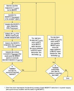
Because a MOSFET's power dissipation depends greatly on its on-resistance (RDS(ON)), calculating RDS(ON) seems a good place to start. But a MOSFET's on-resistance depends on the junction temperature (TJ). In turn, TJ depends on the power dissipated in the MOSFET and the thermal resistance of the MOSFET (TJA). So it's hard to know where to begin. Because several terms within the power-dissipation calculation depend on each other, an iterative process is needed to determine this number (Fig. 1).
This process starts by first assuming a junction temperature for each MOSFET. The same procedure is implemented for both MOSFETs, individually. Both the MOSFET's power dissipation and allowable ambient temperature are calculated.
The process ends when the allowable ambient temperature is at or slightly above the maximum temperature expected within the enclosure that houses the power supply and the circuitry it powers. Making this calculated ambient temperature as high as possible may seem tempting, but it's not usually a good idea. Doing so would require a more expensive MOSFET, more copper underneath the MOSFET, or moving more air by a larger, faster fan—all of which would be unwarranted.
In a sense, this approach entails working backward. After all, the ambient temperature determines the MOSFET's junction temperature—not the other way around. But the calculations required when starting with an assumed junction temperature are easier to accomplish than when starting by assuming an ambient temperature and working from there.
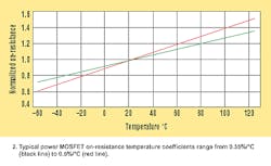
For both the switching MOSFET and the synchronous rectifier, select a maximum permitted die junction temperature (TJ(HOT)) to use as a starting point for this iterative process. Most MOSFET data sheets only specify a maximum RDS(ON) at 25°C. But recently, some have offered maximums at 125°C as well. MOSFET RDS(ON) increases with temperature exhibiting typical temperature coefficients that range from 0.35%/°C to 0.5%/°C (Fig. 2). If in doubt, use the more pessimistic temperature coefficient and the MOSFET's 25°C specification (or its 125°C specification, if available) to calculate an approximate maximum RDS(ON) at your chosen TJ(HOT):
RDS(ON)HOT = RDS(ON)SPEC × \\[1 + 0.005 × (TJ(HOT) - TSPEC)\\]
where RDS(ON)SPEC is the MOSFET on-resistance used for the calculation, while TSPEC is the temperature at which RDS(ON)SPEC is specified. Use the calculated RDS(ON)HOT to determine the power dissipation of both the synchronous rectifier and switching MOSFETs, as described below. The paragraphs that discuss calculating the power dissipation of each MOSFET at its assumed die temperature are followed by a description of the additional steps needed to complete this iterative process.
Synchronous Rectifier's Dissipation: For all but the lightest loads, the drain-to-source voltage of the synchronous-rectifier's MOSFET is clamped by the catch diode during turn-on and turn-off. Therefore, the synchronous rectifier incurs no switching losses, making its power dissipation easy to calculate. Only resistive losses need be accounted for.
The worst-case losses occur at the maximum duty factor of the synchronous rectifier, which happens when the input voltage is at its maximum. Through the use of the synchronous rectifier's RDS(ON)HOT and its duty factor, along with Ohm's Law, you can calculate its approximate power dissipation:
PDSYNCHRONOUS RECTIFIER = \\[ILOAD2 × RDS(ON)HOT\\] × \\[1 >- (VOUT/VIN(MAX))\\]
Switching MOSFET's Dissipation: The switching MOSFET's resistive losses are calculated much like the synchronous rectifier's, using its (different) duty factor and RDS(ON)HOT:
PDRESISTIVE = \\[ILOAD2 × RDS(ON)HOT\\] × (VOUT/VIN)
Calculating the switching MOSFET's switching loss is difficult because it depends on many difficult-to-quantify and typically unspecified factors that influence both turn-on and turn-off. Use the rough approximation in the following formula as the first step in evaluating a MOSFET, and verify performance later on the lab bench:
PDSWITCHING = (CRSS × VIN2 × fSW × ILOAD)/IGATE
where CRSS is the MOSFET's reverse-transfer capacitance (a data-sheet parameter), fSW is the switching frequency, and IGATE is the MOSFET gate-driver's sink and source current at the MOSFET's turn-on threshold (the VGS of the gate charge curve's flat portion).
Once you've narrowed the choice to a specific generation of MOSFETs based on cost (the cost of a MOSFET is very much a function of the specific generation to which it be-longs), the device within that generation that will minimize power dissipation is the one with equal resistive and switching losses. Using a smaller (faster) device increases resistive losses more than it decreases switching losses, and a larger (low-RDS(ON)) device increases switching losses more than it decreases resistive losses.
If VIN varies, you must calculate the switching MOSFET's power dissipation at both VIN(MAX) and VIN(MIN). The MOSFET's worst-case power dissipation will occur at the minimum or maximum input-voltage level. The dissipation is the sum of two functions: the resistive dissipation, which is highest at VIN(MIN) (higher duty factor), and the switching dissipation, which is highest at VIN(MAX) (because of the VIN2 term). An optimal selection has roughly equal dissipations at the VIN extremes, balancing resistive and switching dissipations across the VIN range.
If the dissipation at VIN(MIN) is significantly higher, resistive losses will dominate. In that case, consider a larger switching MOSFET, or more than one in parallel, to lower RDS(ON). But if the losses at VIN(MAX) are significantly higher, consider decreasing the size of the switching MOSFET (or removing a MOSFET if multiple devices are used) to allow it to switch faster.
If the resistive and switching losses balance but are still too high, there are several ways to proceed:
- Change the problem definition. For example, redefine the input voltage range.
- Change the switching frequency, which lowers switching losses and possibly allows a larger, lower-RDS(ON) switching MOSFET.
- Increase the gate-driver current, lowering switching losses. The MOSFET's own internal gate resistance, which ultimately limits the gate-driver current, places a practical limit on this approach.
- Use an improved MOSFET technology that might simultaneously switch faster and have lower RDS(ON) and lower gate resistance.
Fine-tuning the MOSFET's size beyond a certain point may not be possible due to a limited number of devices to choose from. The bottom line is that the MOSFET's worst-case power must be dissipated.
Thermal Resistance: Refer to Figure 1 again for the next step in the iterative process used to determine whether or not you chose the right MOSFETs for both the synchronous rectifier and the switching MOSFET. That step is the calculation of the temperature of the ambient air surrounding each MOSFET that would cause the assumed MOSFET junction temperature to be reached. To do this, first determine the junction-to-ambient thermal resistance (TJA) of each MOSFET.
If multiple MOSFETs are used in parallel, you can calculate their combined thermal resistance in the same way as the equivalent resistance of two or more paralleled resistors. Thermal resistance can be difficult to estimate. While it's relatively easy to measure the TJA of a single device on a simple pc board, it can be hard to predict thermal performance in an actual power supply within a system, where many sources of heat compete for limited dissipation paths.
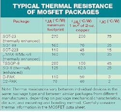
Start with the MOSFET's TJA specification. For single-die SO-8 MOSFET packages,TJA is usually near 62°C/W. For other packages, with thermal tabs or exposed heat slugs, it may range between 40°C/W and 50°C/W (see the table). To calculate the MOSFET's die temperature rise above ambient:
TJ(RISE) = PDDEVICE TOTAL &215; TJA
Next, calculate what ambient temperature would cause the die to reach the assumed TJ(HOT):
TAMBIENT = TJ(HOT) - TJ(RISE)
If the calculated TAMBIENT is lower than the enclosure's maximum specified ambient temperature (meaning that the enclosure's maximum specified ambient temperature would cause the MOSFET's assumed TJ(HOT) to be exceeded), you must do any or all of the following:
- Raise the assumed TJ(HOT), but not above the data sheet maximum.
- Lower the MOSFET power dissipation by choosing a more suitable MOSFET.
- Or, decrease TJA by increasing the air flow or the amount of copper around the MOSFET.
Then recalculate. Employing a spreadsheet simplifies the multiple iterations typically required to settle on an acceptable design.
On the other hand, if the calculated TAMBIENT is higher than the enclosure's maximum specified ambient temperature by a fair amount, any or all of the following optional steps can be taken:
- Lower the assumed TJ(HOT).
- Reduce the copper dedicated to the MOSFET's power dissipation.
- Or, use a less expensive MOSFET.
These steps are optional because in this case, the MOSFET won't be damaged by excessive temperature. However, these steps can reduce board area and cost, as long as the calculated TAMBIENT remains higher than the enclosure's maximum temperature by some margin.
The biggest source of inaccuracy in this procedure is TJA. Carefully read any datasheet notes associated with a TJA specification. Typical specifications assume a device mounted on 1 in.2 of 2-ounce copper. The copper performs much of the power dissipation, and different amounts of copper change TJA dramatically.
For example, the TJA of a D-Pak might be 50°C/W with 1 in.2 of copper. But with copper underlying just the package footprint, the TJA more than doubles (see the table again). With multiple MOSFETs in parallel, the TJA mostly depends on the copper area to which they're mounted. The equivalent TJA for two devices can be half that of one device, but only if the copper area also is doubled. That is, adding a parallel MOSFET without also additional copper halves RDS(ON) but changes TJA much less.
Lastly, TJA specifications assume that no other devices contribute heat to the copper dissipation area. At high currents, every component in the power path, even pc-board copper, generates heat. To avoid overheating the MOSFETs, carefully estimate the TJA that your physical situation can realistically achieve. Study the selected MOSFET's available thermal information; investigate whether or not space is available for additional copper, heatsinks, and other devices; determine if increasing the air flow is feasible; see if other devices contribute significant heat to the assumed dissipation path; and estimate excess heating or cooling from nearby components and spaces.
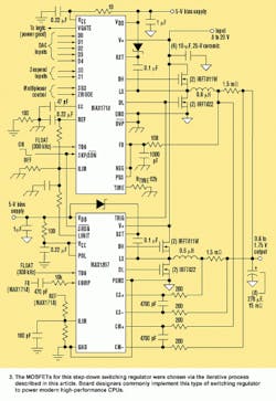
A Design Example: The CPU core supply shown in Figure 3 delivers 1.3 V at 40 A. Two identical 20-A power stages operating at 300 kHz supply the 40-A output current. The MAX1718 master controller drives one stage, while the MAX1897 slave controller drives the other. This supply's input range spans 8 to 20 V, with the specified maximum ambient temperature of the enclosure at 60°C.
The synchronous rectifier comprises two IRF7822 MOSFETs in parallel, with a combined maximum RDS(ON) of 3.25 mO at room temperature, and about 4.7 mO at 115°C, the assumed TJ(HOT). With a maximum duty factor of 94%, a 20-A load current, and the 4.7-mO maximum RDS(ON), these paralleled MOSFETs dissipate about 1.8 W. Supplied with 2 in.2 of copper to dissipate that power, the overall TJA should be about 31°C/W. The temperature rise of the combined MOSFETs will be about 55°C, so this design will work with an ambient temperature of up to about 60°C.
Two IRF7811W MOSFETs in parallel, with a combined maximum RDS(ON) of 6 mO at room temperature, and about 8.7 mO at 115°C (the assumed TJ(HOT)), make up the switching MOSFET. The combined CRSS is 240 pF. The MAX1718's (and MAX1897's) 1-O gate drivers deliver about 2 A. At VIN = 8 V, the resistive losses are 0.57 W, and the switching losses are approximately 0.05 W. At 20 V, the resistive losses are 0.23 W, and the switching losses are approximately 0.29 W. Total losses at each operating point roughly balance, and the worst-case total equals 0.61 W at the minimum VIN.
Because this level of power dissipation isn't high, we can provide this pair of MOSFETs with under 0.5 in.2 of copper area, achieving an overall TJA of about 55°C/W. This still enables operation up to an ambient temperature of 80°C with a 35°C temperature rise.
The copper areas in this example are required for the MOSFETs alone. If other devices dissipate heat into those areas, more copper area will likely be required. If space isn't available for this additional copper, reduce the total power dissipation, spread the heat to areas of low dissipation, or use active means to remove heat.
Thermal management is one of the most difficult areas of high-power portable design. That difficulty makes the iterative process outlined above necessary. Although this process should get the board designer close to the final design, lab work must ultimately determine whether the design process was sufficiently accurate. Calculating the thermal properties of the MOSFETs and ensuring their dissipation paths while checking those calculations in the lab helps ensure a robust thermal design.
About the Author
Comment About the Article
To join the conversation, and become an exclusive member of Electronic Design, create an account today!

Leaders relevant to this article: