Ethernet Port Protection Requires Smart Design And Test Strategies
Good design practice for Ethernet ports needs overvoltage and overcurrent protection devices in addition to proper component creepage distances and electrical trace clearances. After calculating a printed-circuit board’s (PCB’s) creepage and clearance distances, we must select protection devices for both sides of the Ethernet I/O connections, i.e., the line (RJ-45) and driver (physical layer, or PHY) sides.
Ethernet protection devices typically are multi-channel transient-voltage suppressor (TVS) diode arrays, which provide the lowest clamping voltages available among the various protection technologies. They’re available in a wide selection of small-form-factor packages, ranging from single devices for single-port protection to multiple devices to protect multiple lines, all within a single package to minimize footprint requirements.
TVS diode arrays are used when: the PHY circuits being protected require low clamping voltages, low capacitance from 0.4 pF to 5 pF typical, and low leakage current around 0.1 μA to 25 μA; when multiple lines must be protected and board space is limited; and when transients appear due to a variety of threats.
TVS diode arrays with appropriate characteristics must be selected for the four main overvoltage electrical threats: lightning induced surges, electrostatic discharge (ESD), electrical fast transients (EFTs), and cable discharge events (CDEs). Low capacitance is especially important in these devices to avoid signal distortion, particularly in gigabit Ethernet circuits.
The TVS diode arrays must be connected to ensure adequate suppression of these threats. They should be placed as close as practicable to the entry point of the electrical threat while using the same ground reference as the PHY being protected.
Threat suppression may require other design considerations, such as using fuses and connecting a power supply line bypass capacitor to ground near the PHY power input pin to ensure proper power filtering. A PCB prototype should be tested to IEC or other pertinent standards to verify the proper creepage and clearance of the PCB layout. This will help prevent arcing during power fault and surge conditions and allow the TVS diode arrays to effectively clamp these events.
Creepage And PCB Trace Clearances
To prevent dielectric breakdown and sparking on the Ethernet PCB, the line side and ground should have sufficient creepage and trace clearances. Creepage is the shortest path between two conductive parts, or between a conductive part and the bounding surface of the equipment, measured along the surface of the insulation.
Adequate creepage distance protects against tracking, a process that produces a partially conducting path of localized deterioration on the surface of an insulating material as a result of electric discharges on or close to an insulation surface.
The degree of tracking depends on two major factors: the comparative tracking index (CTI) of the PCB material and environmental factors such as altitude, humidity, and contaminants. The CTI provides a numerical value of the voltage that will cause failure by tracking during standard testing. IEC 112 provides a fuller explanation of tracking and CTI.
Clearance is the shortest distance between two conductive parts, such as circuit board traces, or between a conductive part and the bounding surface of the equipment as measured through air. Clearance distance helps prevent dielectric breakdown between parts caused by the ionization of air. Dielectric breakdown level is also influenced by the PCB CTI rating, relative humidity, temperature, and pollution degree in the operating environment.
Board-level designers usually consider peak working voltage in creepage and clearance distance calculations, but electrical transients also need to be considered. Some of these transients can be as high as a few thousand volts.
Lab tests have shown that to withstand 2 kV of transient voltage, an FR4 circuit board trace spacing should have a separation of at least 25 mils. However, this clearance distance may be too great to be reasonable for Ethernet board layouts where normal spacing of the Ethernet pair is 5 mils with 5-mil trace widths.
This is another important reason for transient protection: to reduce high voltages so spacing can be much smaller, i.e., high voltages are suppressed due to the clamping action of the TVS diode array. In UL 60950-1, Table 2K shows minimum clearance for 2.8 kV as 8.4 mm (330 mils) and 1.4 kV as 6.4 mm (252 mils).1 But this is for a steady-state voltage, not a fast rising dv/dt that characterizes surge events. So, maintaining potential differences between traces using the TVS is vital to board layout.
Understanding the nature and polarity of transient events will help guide designers to the best Ethernet port protection solution. This comprehension will provide insights on how to properly locate and connect the protection device.
Lightning Induced Surges
Most standards, recommendations, or regulations will define a common-mode (longitudinal) surge requirement as a minimum resistibility level. These common-mode events can be converted into differential (metallic) events. As a result, some of these standards, recommendations, and regulations may also define a differential surge requirement resistibility level. GR-1089-Issue 6,2 IEC 61000-4-5, and ITU K20/21 cover waveform generation and testing procedures.
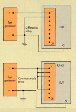
Figure 1 shows test setups for these two cases. In the differential mode, two conductors or pins (i.e., J1 and J2) are connected between the positive and negative test equipment terminals, so the surge event inserted at the RJ-45 port appears only between these two conductors.
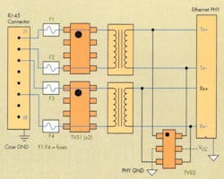
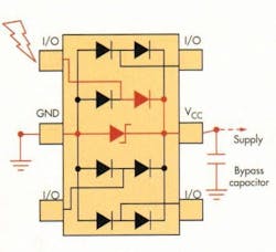
Most of the energy will be dissipated in the line side protection devices shown in Figure 2 as TVS1 (x2). However, some of the energy will also be coupled through the transformer creating either a common-mode or differential event on the driver side of the transformer.
For common-mode testing, the individual conductors or data lines themselves will be tested with respect to ground. The waveform generator output will be connected to all of the conductors or pins (J1, J2, J3, and J6), and its ground reference will be tied to the PCB ground reference. It’s important to note that this may not be the same reference point as the PHY GND, depending on how the application is designed.
Many times the PHY GND is isolated from the analog ground of the PCB. This is one of the advantages of using the coupling transformer. In this case, very little energy should be coupled across the transformer. But due to inter-winding capacitance, the combination of TVS1 and the transformer won’t prevent all of the energy from being transferred to the PHY side. This energy will be capacitively coupled through the transformer’s magnetics to its driver side, and it may appear as either a common-mode or differential event, or both, to the Ethernet PHY.
To comply with IEEE 802.3 standards for isolation, the line side protection device TVS1 in Figure 2 may not have its ground pins (2, 3, 6, and 7) tied to ground. According to IEEE 802.3 references to UL-60950-1, though, this grounded connection may be allowed. TVS2 will always have its I/O pins tied to the differential pairs as shown in Figure 2.
However, unlike the line side protector, this device can have its ground pin connected to the local ground plane and its reference pin connected to the PHY VCC. (Littelfuse recommends this configuration.) If the ground pin were not connected, then TVS2 would become a differential only protector and could potentially allow damaging common-mode events to pass through to the PHY unclamped.
Electrostatic Discharge
ESD is a common threat to small circuit traces and components. It’s caused by the transfer of static electrical charge from a body to an electronic circuit, and it isn’t uncommon for the transient to have a peak as high as 15 kV. In less severe cases, ESD may result in faulty circuit operation or latent defects that later progress to outright failure.
ESD suppressors must have very fast response times and repeatedly handle high peak voltages and currents for short durations. TVS diode arrays are clamping devices that limit the transient to a set value. The low dynamic resistance of the TVS enables it to clamp these high-voltage ESD events to a very low level (think I × R) once its clamping threshold is exceeded. The TVS device will stop conducting once the transient voltage drops below the device’s reverse standoff voltage.
Equipment being evaluated for immunity to ESD, as per the IEC61000-4-2 standard, will have testing conducted via contact and air discharge. There are numerous methods of injecting ESD in a test, such as those described in IEC61000-4-2. But in all cases, the ESD pulses appear as common-mode events to the RJ-45 connector line side point since this discharge event is referenced to ground. Protective devices are connected and testing conducted according to the discussion on common-mode events earlier.
Electrical Fast Transient
Equipment being examined for immunity to EFT per IEC61000-4-4 is very similar to the testing done for common-mode lightning surges. In the more typical configuration shown in Figure 3, all the conductors (or pins) are connected to the positive terminal of the test generator and “surged” with respect to GND.
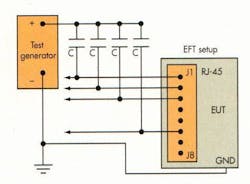
Coupling capacitors aren’t needed unless it’s a power over Ethernet (PoE) application, in which case a capacitance value of about 33 nF should be sufficient. If the data lines are well balanced, there will be little to no differential energy between the pairs. But again, the transformer’s coupling capacitance will transfer the common-mode energy to the driver side, albeit at a reduced level.
Cable Discharge Event
Cable discharge event (CDE) differs from ESD in the way it’s created and in its waveform characteristics. CDE events typically occur when a PVC-covered CAT5 unshielded twisted-pair (UTP) cable is pulled on a nylon carpet or over tile flooring, which can cause charge to build up on the cable. Similarly, charge also can build up on a cable when it’s pulled through a conduit or dragged over other network cables. The twisted-pair cable behaves like a capacitor by storing the charge.
However, the charge buildup only occurs when the cable is un-terminated and the charge isn’t immediately dissipated, i.e., both ends of the cable aren’t plugged into a system. Newer CAT5 and CAT6 cables have very low dielectric leakage and tend to retain charged for a long period. Charge retention time is increased in an environment where there is low relative humidity.
When a charged UTP cable is plugged into an RJ-45 network port, there are many possible discharge paths. This transient current takes the lowest inductance path, which could be at the RJ-45 connector, between two traces of a PCB, in the transformer, through the Bob Smith ac termination, or through the silicon device. Thus, damage can occur to the Ethernet transceiver or any of the devices mentioned.
The amount of charge depends on the length of the cable (Fig. 4). Studies have proven that up to several hundred volts of charge can accumulate on an unterminated twisted-pair cable. Extra CDE precautions should be taken with systems that have cable lengths greater than 60 m.
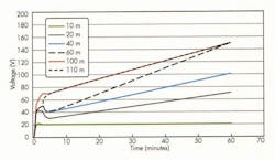
A CDE waveform is unlike any of the other threats described earlier. It can be differential or common-mode, depending on the coupling mechanism. While it can have wide variations, its general characteristic is high energy that exhibits both voltage and current drive. The waveform is spread out in time over hundreds of nanoseconds with rapid polarity reversals. In this experiment, the PHY’s transmitter was destroyed and unable to transmit packets on the network.
A system designer can maximize protection against CDE through good layout practices (component creepage and trace clearances) as described earlier. TVS diode arrays help divert energy away from ICs and other sensitive components. The transformer circuit will also help protect against common-mode transients.
Keep in mind that the IEEE 802.3 standard calls out isolation voltages of 2.25 kV dc and 1.5 kV ac to prevent connector failures that can be caused by the high voltages generated from CDEs. To prevent arcing during these events, these isolation requirements apply to the RJ-45 connector as well as to the isolation transformers. According to the UL-60950-1 references in this IEEE 802.3 document, any grounded protection may be removed for any isolation testing but then reinstalled for any surge testing.
The TeleLink fuses (see the line side fuses in Figure 2) between the coupling transformer and the RJ-45 connector protect the circuit against overcurrent surges. Power cross events and surge coupling from nearby ac lines typically cause these surges.
Protection Device Circuit Connections
Most circuit connections for a TVS diode array protective device were described earlier under Lightning Induced Surges, which emphasized grounding techniques to allow dissipation of transient energy. The I/O connections would be as shown in Figure 2.
The remaining pin commonly found on most TVS diode arrays is labeled VCC. This pin should be tied to the Ethernet PHY power supply rail such as 5 V, 3.3 V, etc., as shown for the driver (PHY) side device (TVS2) in Figure 2. Care should be taken to make sure the protection device’s standoff voltage or VRWM is above the supply voltage to prevent steady-state activation of the protection.
TVS diode arrays employ multiple semiconductor technologies, permitting them to provide two types of protection (Fig. 5). First, they absorb transients with diodes that steer the current away from the circuit or components being protected. Second, an avalanching or zener diode clamps the voltage to a safe level.
TVS diode arrays are characterized for a clamping voltage level during specific surge current waveform testing. This clamping voltage must be low enough to protect the Ethernet PHY but not so low it interferes with normal steady-state signaling.
By connecting the VCC pin of such a device to the power supply, the TVS diode array will achieve a lower clamping voltage due to the additional current paths provided by the power supply and the bypass capacitor (See the red lines in Figure 6.) It can be seen as a resistive divider where the transient enters through the steering diode and takes two paths: one to ground via the internal TVS and one to ground through the bypass capacitor and power supply.
Conclusively, connecting the VCC pin to the power supply will result in better clamping performance, providing overall better protection for the Ethernet PHY depending on the proper placement of the bypass capacitor. If this bypass capacitor is not correctly chosen and placed, then connecting to the power rail could become a source of transient damage.
It should also be noted that some diode arrays have an internal TVS diode that exhibits a snap-back characteristic and could therefore be damaged if the power supply is connected externally. The VCC pin of the TVS diode array shoudn’t be connected in these cases.
Another benefit of biasing the VCC pin is that it will lower the capacitance from I/O to GND instead of leaving it floating or disconnected. This is important for the prevention of signal loading and intermodulation distortion, particularly in Gigabit Ethernet circuits. The datasheet for the particular device being used to protect the Ethernet PHY should be consulted so the designer knows the value of this capacitance, which partly depends on the VCC bias level.
Device Selection Parameters
Besides low capacitance, another characteristic to be considered in Ethernet protection device selection is dynamic resistance, (RDYN) or the effective silicon resistance of the TVS device when it’s active or in its on-state. RDYN should be low to ensure fast response and low clamping voltages, i.e., low I × R and R × C factors.
Additional device parameters to be evaluated include reverse standoff voltage (VRWM), peak surge voltage, peak surge current rating (IPP), ESD rating, reverse leakage current (IR), clamping voltage (VC), and peak pulse power rating (PPK).
In addition to these selection criteria, protective devices must also fit within the circuit board real estate and be available in a package configuration that’s suitable for available mounting and soldering equipment. The primary consideration is selecting a TVS diode array that will protect the Ethernet circuit board and its components and can do so repeatedly without failure. Protection device manufacturers supply a wealth of application support to help in making these selection decisions.
Reference
About the Author
Comment About the Article
To join the conversation, and become an exclusive member of Electronic Design, create an account today!

Leaders relevant to this article: