PCB Designers Need to Know These Panelization Guidelines


This article provides common-sense printed-circuit-board (PCB) processing edge and array guidelines that should give most assemblers a good chance at efficiently populating the PCB assemblies (PCBAs) as designed. These guidelines are intended for PCB designers, who must understand the basics of assembly methods (including panelization concepts) applicable to their designs if there’s any hope they will consistently turn out manufacturable board designs. These are also targeted at the PCBA process technician trainee, so he or she will know what to ask for in a PCB array design.
Guidelines spell out when to create arrays or add processing edges; the proper sizes for arrays and processing edges; the type of breakout design that should be used under given circumstances; and how to arrange breakouts to prevent damage to individual PCBs when breaking them out of the array or while removing processing edges.
This article uses the terms array and panelization interchangeably, whichever seems to fit best at that time. It’s also common to use the term “matrix” for an array of PCBs. It can get confusing, because the word “panel” is reserved for the standard-size laminate piece used by the PCB fabricator, whereas the word “panelization” indicates a method of designing an array of PCBs into a single processing piece for the PCB assembler.
It’s impossible to come up with a set of hard rules for all due to the differences in machine technologies from one assembly shop to another. In addition, the PCB construction and thickness can play a major role in what rules to use. To satisfy a variety of assembly shops and PCB construction technologies, the PCB design has to be more robust—stronger panels, more clearance of all types, more robust board finishes, etc. If you have a captive assembly shop, you will have the flexibility to adjust some of the guidelines, according to the assembler’s unique capabilities, when product design density dictates the need.
PCB Processing Edge or PCB Array
Small boards
Most production machinery, paste printers, pick-and-place machines, AOI equipment, selective soldering machines, wave-solder machines, transfer conveyors, etc., cannot process boards with less than a 2.0-in. (50.8mm) conveyor width. So when the longest side of a rectangular PCB is less than 2.0 in., you must either add processing edges to make it bigger or create an array of boards, or a combination of the two.
Odd-form boards
When a PCB needs to fit into an odd-form space and doesn’t have two parallel edges for processing on conveyors, one must somehow add the necessary processing edges. These make for some pretty interesting and complex array designs, keeping in mind how the boards will be depanelized and how board cost is minimized by making them fit well on the fabricator’s standard processing panel. These considerations are covered below.
Note: You do have the option of using an adjustable or custom-made board carrier, but these options are pretty expensive and cumbersome. They can also be maintenance-intensive and use up significant floor space.
Board-Array Dimensions
You should design your PCB array to secure the benefits of running multiple boards through your processes, while yielding the maximum number of boards from the PCB fabricator’s standard processing panel. Every cut in the array that’s made to facilitate future PCB breakout will weaken the panel somewhat. Therefore, you must also limit the size of the array to prevent PCB-array weakness, which can cause vibration in the pick-and-place machine and sagging in the wave-solder machine.
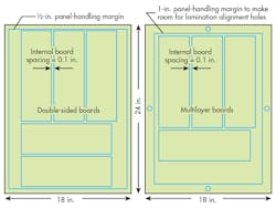
The typical PCB manufacturer runs a standard panel size of his choice, very commonly 18 × 24 in. They will want a 1/2-in. perimeter clearance for handling the panels when processing double-sided boards and a 1-in. clearance when processing multilayer PCBs. On an 18- × 24-in. panel, this translates to 17 × 23 in. of usable panel space for double-sided and 16- × 22-in. inch panel space for multilayer boards. They will need about 0.1 in. of routing space between board arrays, so this is also unusable panel space. A number of “panel calculators” are available for use to help maximize the board count you get from the fabricator’s standard panel; however, if you don’t get 70% usage, you should try harder (Fig. 1).
The other item to consider when designing the panel size is to keep the conveyor width changes to a minimum. This is especially important in the low-quantity, high-mix world in which I live. If you’re running millions of identical boards down a line, then this isn’t a big concern.
In one example of limiting the conveyor width changes, the following array widths were developed to use the 24-in. dimension of the fabricator’s panel efficiently with a 1-in. perimeter handling clearance:
W = 3.75 in., L ≥ W
W = 7.25 in., L ≥ W
W = 10.75 in., L ≥ W
The length of the array is then subject to the 16-in. limitation of the 18-in. panel edge.
Panelization Methods
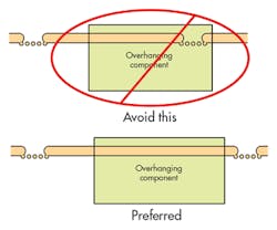
The design of the board—namely how much component clearance is provided on the edges, whether sensitive SMT components are close to an edge, and whether or not connectors or other components hang over an edge—will limit the choices of panelization breakout methods from which to choose. Sometimes a combination of methods is appropriate to secure the PCB-array strength, while providing a viable breakout method.
To improve strength, increase the board count on the fabricator’s panel, and facilitate automated depaneling, arrays can be designed with solid tabs between boards in just about any orientation. The depaneling method for this kind of panel is either a depaneling router or a laser-cutting machine. The former creates vast amounts of dust, noise, and vibration, and requires firm holding fixtures. The latter is capital-intensive and limited to board thicknesses of about 1 mm. Still, these methods have their place in the high-volume market and aren’t subject to many of the restrictive guidelines to be outlined later.
The solid tabs between boards can be removed with a hook-shaped blade tool, but this process can be troublesome. Even with very little clearance of the blade in the slot between boards, it can rotate and take a bite out of the good part of the board. If the blade-cutting edge is tapered to prevent board damage, it leaves a little of the tab protruding from the good board. It’s also a very inefficient process.
The two preferred depanelization methods for the low-volume/high-mix arena are V-grooves and perforated tabs. Tabs and V-grooves are pretty well covered in the IPC standards.
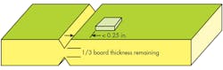
V-Groove Panelization Method
Generally speaking, this calls for cutting 1/3 the thickness of the board from the top and 1/3 the thickness from the bottom, collinear with the top cut, with a 30- to 45-degree circular cutting blade. A machine is needed to depanel it, as the remaining 1/3 of the board thickness left intact is surprisingly strong, and breaking it off by hand would put severe stress on the PCB.
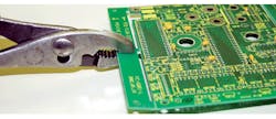
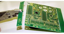
Many prefer the V-groove method (Fig. 2) where possible (in which no components hang over the edge), because it’s more efficient and produces less surface stress when using a properly designed machine known as a “pizza cutter.” Also, the pizza-cutter-type depaneling machines for V-grooves are inexpensive, last forever, and require very little adjustment and maintenance. Furthermore, they’re portable—you can mount the depaneling machines on a small cart and easily move them around the shop wherever they’re needed.
However, this is the most restrictive method of panelization. For example, you can’t use a V-groove breakout method where components are hanging over the edge. Even if they’re too close to the edge of the board, you can’t use this method unless you’re cutting a straight line all the way through the PCB array.
To clear the circular cutting blade, you must maintain 0.05-in. clearance from components to the center of the V-groove score, taking into consideration component size and mounting variations. Tall components, such as radial capacitors, radial inductors, and power-dissipating radial ceramic resistors, would have to be spaced greater than 0.05 in. (nominal) because of position variation, whereas connectors and other low-profile parts may be placed at 0.05-in. clearance.
Surface-mount multilayer ceramic chip capacitors (MLCCs) must be oriented with the long side parallel to the V-groove cut if less than 0.25 in. (6.35 mm) away from the score line and kept 0.119 in. (3 mm) away regardless. This becomes more important with the larger-size caps and with certain cap dielectrics. The surface stress, caused by forcing the depaneling blade into the V-groove, transfers through the board surface to the rigid solder joints, and then to the component bodies. This can fracture them if they're too close to the V-groove. Orienting the long edge of the capacitor body parallel to the edge minimizes the risk of body fracture (Fig. 2, again).
V-grooves can also weaken a PCB array, which is very undesirable when the array must go through a wave-solder machine. The surface tension of the solder wave, pulling down on the preheated PCB material, is exacerbated by V-grooves in the array. When the board is pulled down, the protruding leads tend to run into, and sometimes get hung up, on the wave-solder baffle.
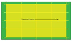
In the case of a rectangular PCB, you would strengthen the array by “jump scoring” on the shorter, or leading and trailing, edges (Fig. 3). Since the V-groove blade is circular, you must cut beyond the edge of the board to achieve a full-depth V-groove at the edge of the board. Running the cut 1/4 in. past the edge of the PCB, halfway through a 1/2-in. breakaway edge, will leave enough of the leading and trailing edges to strengthen the array and minimize the pulling down effect of the wave, while achieving the desired full depth V-groove cut on the board.
When jump scoring is used, the depaneling operators must be instructed to remove the leading and trailing edges before trying to separate the boards. You may get some push back from the PCB fabricator, but it gives you a stronger array. Give the fabricator a break by not dimensioning the end of the jump score. It’s hard to control, and you don’t know the V-groove cutting-blade diameter. So you don’t know exactly where the cut will end.
Note: The V-groove method is undesirable if a “clean,” smooth board edge is required, but this is rarely the case.
Breakaway-Tab Panelization Method
When V-grooves can’t be used, design PCB arrays, leaving perforated tabs routing space between PCBs. Keep traces and surface-mounted parts 1/8 in. or about 3 mm away from the perforation holes in the tabs to avoid damage from splintering and surface stress during board separation. Keep the SMT MLCCs 1/4 in. (6.35 mm) away from the perforated-tab holes. Standard router size is 3/32 in. or 2.5 mm in most fabrication houses, and you want to design a spacing that requires a single pass of the router bit. Where array weakness was a consideration for V-groove designs, it’s doubly so for perforated-tab arrays.
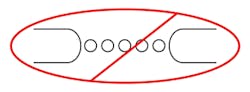
A five-hole perforation pattern is standard for breakaway tabs. Three-hole patterns, which are for knockouts, may be used where trace or component edge clearance is limited and where tabs must be placed under overhanging parts. The three-hole breakouts, being much weaker, must be spaced closer together than the five-hole breakouts.
Removable knock-outs are required to fill holes with area greater than or equal to 0.6 in.2, to prevent the solder wave from running onto the top of the board. In the case of a relatively small, rectangular knockout, a single five-hole breakout tab may be placed on any one side. Since PC boards will sag in the middle over the wave, knockouts are more important toward the middle of the board and less important toward the edges. If the wave-solder process isn’t necessary, the knockouts aren’t required.

The breakout-tab specifications, adapted from IPC-7351 (Fig. 4), are designed to prevent the leftover material from the tab perforations from protruding past the PCB edge after breakout. This may cause some headaches for the PCB designer when running traces near the board edge, but it can usually be accomplished if kept in mind from the beginning of the board design.
Perforated holes, centered in the routed cutout, will cause unwanted side board protrusions (Fig. 5).
Three-hole perforated tabs are used for knockouts and for board edges when there’s not enough room for five-hole perforated tabs. A rectangular knockout can be designed with a five-hole perforated tab on any single edge (Fig. 6).

Do not place breakaway tabs under overhanging components (Fig. 7).
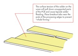
Tabs must be placed as close to the ends of the panel as possible to prevent "whale finning" (Fig. 8) and thereafter, every 2 to 3 in. for five-hole pattern or 1.5 in. for three-hole perforated tabs. Three-hole pattern breakouts are used on board edges where space and clearance prevents use of five-hole breakouts.
Three-hole pattern breakouts are used on board edges where space and clearance prevents use of five-hole breakouts.
The breakaway panels must be designed so that all tabs broken at one time are collinear. Another way to state it is that the break axis must be collinear with the tab hole perforations involved in any one break. If the tab perforations aren’t collinear during the breaking operation, some tabs will experience a force perpendicular to the board surface, causing a tearing action on the surface lamination (Fig. 9).
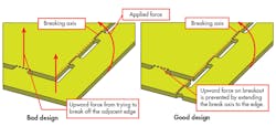
It could be just the solder-mask layer that delaminates and gets separated from the traces, or it could actually be the surface layer of the board that tears and pulls up any traces with it. This is a main complaint against the perforated-tab method of panelization. At AMETEK, we have found a breaking method that will never damage a board, which is described below. In practice, though, this method IS NOT foolproof.
Combining Panelization Methods
Putting the guidelines together for the V-groove and perforated-tab panelization methods, let’s look at two array designs for the same board (Fig. 10).
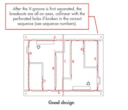
The good design reduced the board count on the fabricator’s panel. However, it was well worth paying slightly more for the PCBs in order to prevent the board damage that kept occurring during breakout and the problems with the wave-solder overflow.
Critical Instructions for Breaking Out Boards with Perforated Tabs
No matter how well you design a perforated-tab PCB array, the possibility exists for tearing or splintering the solder-mask layer, or the active surface layer, of the PCB if a poor method of break out is used. The following is a safe method of breaking out perforated-tab arrays, to both minimize PCB damage and the stresses transferred across the PCB’s surface to the components during breakout (Figs. 11 and 12).
Panel-Strength Considerations for Multiple Board Arrays
The main reasons for maintaining overall panel strength is to avoid vibration in the pick-and-place machine and droop during wave soldering and selective soldering. The rules outlined below may be relaxed by 50% if the panel will not be subjected to any form of through-hole machine soldering. They also may be relaxed if the panel will be soldered on a supporting pallet. Following are some guidelines to assure sufficient panel strength to withstand processing stresses.
V-groove scoring or breakout tabs with routing between boards cause significant reduction in panel strength. The number of V-grooves or routings between boards on a multiple image pallet must be limited, depending on:
• Board material and thickness
• Weight of parts to be installed on the board
• Whether or not the boards will be processed through soldering machines, using a rigid soldering pallet
Multiple board panels must be designed in a way to provide leading and trailing unscored stiffener edges. Use jump scoring, as described earlier in the article, as necessary. If heavy parts must be hand-soldered because they can’t withstand automated soldering processes or because they’re on the bottom side of the board, they’re not a factor in panel design decisions.
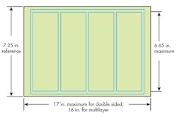
For FR4 or HTFR4 PCBs greater than or equal to 0.06 in. (1.5 mm) thick, allow no more than five boards, side by side, up to 1.5-in. board width, four boards up to 2.5-in. board width, three boards up to 4-in. board width, and two for boards up to 7.5-in. board width. Boards up to 6.65 in. long may be turned 90° on the panel and placed side by side along the long axis of the array to fit within the standard 7.25-in. width. This only makes sense if the resulting panel is longer than it is wide, so you can add boards to the array to utilize the fabricator’s panel efficiently (Fig. 13).
You may also attempt to rotate longer boards, up to 10 in. long, 90° to fully utilize the fabricator’s panel. However, that usually results in excessive array droop during through-hole machine soldering. Rotating the longer boards is more practical on thicker, more robust PCBs. When designing the standard, 0.09-in.-thick PCBs, the board count can increase in the arrays above these guidelines.
For FR4 or HTFR4 PCBs less than 0.06 in. (1.5 mm) thick, allow no more than three boards side by side, up to 1.5-in. board width, and two boards, up to 3-in. board width. Note that these panels will be extremely fragile and still not be wave-solderable without being supported by a wave pallet.
Another consideration during PCB-array design, to avoid drooping in processing machines, is the weight of the parts on the board. If the boards will have heavy magnetics (greater than a half a pound or 1.1 kg) or other massive parts on them, it’s best not to put multiple boards on a panel. Two boards with heavy parts may be placed side by side if the resulting panel width is no more than 7.25 in. In this case, it’s best to specify a thicker PCB, say 0.09 in.
Miscellaneous Considerations
Odd-shaped PCBs: Odd-shaped boards may be rotated with respect to each other to reduce PCB raw material waste, thus reducing board cost. It’s acceptable to alternate the images, 90° to 180° from each other, to realize the savings in PCB material, as long as you don’t violate the rule about breakout tab perforations being collinear with each breakout axis.
Tooling holes: To facilitate bed-of-nails testing, provide tooling holes near any three corners of the board arrays on the breakaway processing edges. Tooling holes are typically 0.125 in., +0.004/-0.00, and are unplated. Also, tooling holes are usually placed about 5 mm from the edge of the board-array edges.
Fiducial marks: Arrays that contain PCBs with surface-mounted parts must have fiducial marks, typically one near each tooling hole. There are many choices for fiducial-mark formats, so you should consult your assembler for their preference. The edges of the fiducial marks must be at least 0.157 in. (4 mm) from the board edges so that they don’t get obscured by conveyor top clamps in the processing machines with fiducial-alignment camera systems. The array processing-edge fiducial marks don’t preclude the necessity of providing fiducial marks on the individual boards within the array.
Conclusion
No designer can afford to ignore such PCB panelization considerations. PCB-array designs may dramatically impact, either positively or negatively, the PCB assembly process. The various considerations are complex and will be affected by PCB geometry, as well as the myriad of machine capabilities of countless PCB assembly service suppliers. PCB cost can also be significantly affected by the array design.
The above guidelines aren’t set in cement, but they work for us as good practice in AMETEK production applications. You should always try to connect with your PCB assembly service to become familiar with its capabilities and machine process requirements. But since this is often impossible during the design phase of PCBs, try to design on the robust side to improve your chances of achieving an efficient assembly process.
About the Author
Jack Lucas
Senior Manufacturing Engineer, PC Board Assembly Department
Jack Lucas is the Senior Manufacturing Engineer for the PC Board Assembly Department of AMETEK Programmable Power in San Diego, Calif. He has been involved in the PC board assembly process since 1969.
Comment About the Article
To join the conversation, and become an exclusive member of Electronic Design, create an account today!

Leaders relevant to this article: