SmartNIC Architectures: A Shift to Accelerators and Why FPGAs are Poised to Dominate
This article is part of the Communication and System Design Series: Have SmartNIC - Will Compute
Generic network interface cards (NICs) are built around a single application-specific integrated circuit (ASIC) engineered to be an Ethernet controller. Good examples of these are the ConnectX line by Mellanox, the Broadcom NetXtreme, or the Xilinx XtremeScale. Often, these chips are further optimized around a second design objective; for example, the ConnectX line also supports Infiniband, while the XtremeScale is focused on kernel bypass. These controllers are excellent at what they do, they represent the finest in the industry, but they are not SmartNICs.
For the purpose of this article, we’re defining a SmartNIC as a NIC that allows for additional software that can be loaded into the NIC at some point after it’s purchased to add new features or support other functions. Much like when you buy a smartphone and later install apps from that vendor’s app store.
The capability to load future code into a NIC, making it a SmartNIC, requires additional computational power and onboard memory not found in generic NICs. Most SmartNIC approaches start with a foundational Ethernet controller either on the chip in silicon, as firmware, or as a separate chip on the adapter. Then one of three approaches below are used to make an otherwise generic NIC smart by increasing its computational power through the addition of a:
- Collection of many Arm cores; some call it clustering, others use the term grid or tiles.
- Flow processing cores (FPCs), which are custom-designed network processors, often P4.
- Field-programmable gate array (FPGA), programable logic.
Many of these SmartNICs will often use one or more Arm cores for control-plane management within the NIC. Some even allow for loading a modified Linux kernel into one or more of these cores. These Arm cores typically handle loading code into the other processing elements, gathering statistics and logs, and watching over the health and configuration of the SmartNIC. They don’t touch any of the network packets, and they often run “out-of-band,” meaning that they can’t be accessed via “normal” network interfaces or PCIe commands.
Also, the cores should only accept duly signed firmware bundles over previously secured interfaces. Beyond architectural sketches, we won’t call out these control-plane Arm cores below, as they’re required plumbing. And on their own, they don’t generally add value to the feature set offered by that SmartNIC.
Product Comparison
To understand how SmartNICs differ from Generic NICs, let’s take a dive into the leading SmartNIC products from four of the biggest NIC companies on the planet, and two upstarts to see what improvements they offer. The six companies selected are Broadcom, Intel, Nvidia (previously Mellanox), Netronome, Pensando, and Xilinx. We’ll also throw in some insights on a stealth project currently called Fungible.
Broadcom
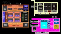
Broadcom is the undisputed leader in the commodity Ethernet NIC controller market. So, when it came time to assemble its Stingray SmartNIC and enter the fray, the company went with a single-chip approach (Fig. 1). Single-chip SmartNIC solutions are always less costly to produce at the board level than many chip boards by other competitors.
Broadcom designed the NetXtreme-S BCM58800 chip at the heart of Stingray by starting with the logic from its NetXtreme E-series controller as a base. Then eight Arm v8 A72 cores clocked at 3 GHz were laid down in a cluster configuration. At 3 GHz, these may be the fastest SmartNIC Arm cores. Also, Stingray can be configured with up to 16 GB of DDR4 memory. Next, some logic was mixed in to offload encryption at up to 90 Gb/s as well as offloads for storage processing like erasure coding and RAID.
Finally, Broadcom added its somewhat mysterious TruFlow technology. This is a configurable flow accelerator for moving common network flow processes into hardware; we believe the company is using a P4 processor. This frees the Arm cores to focus on more computationally intensive tasks at both the flow and packet level. From what’s published, TruFlow seams to offload tasks like Open vSwitch (OvS) in hardware. The company also claims that TruFlow implements many of the classic software-defined networking (SDN) concepts like classification, matching, and action in hardware. So, Stingray has two programable components, TruFlow and a cluster of four 3-GHz, dual-core Arm v8 A72 complexes.
Broadcom is preparing to move Stingray to the 7-nm process later this summer, which will enable scaling from eight to 12 cores. Understanding the complexity of the product it’s providing, the company also offers a Stingray developer’s kit for both SmartNIC application development and storage controller development. This is less common than you might think, and it’s a necessary component for a complete SmartNIC product offering.
Nvidia
Nvidia defined graphical processing units (GPUs), which has become the darling accelerator of choice in high-performance computing (HPC). Earlier this year, Nvidia finally closed on the purchase of Mellanox for $7 billion. In its quest to own the HPC market, the company has picked up the premier Infiniband interconnect vendor, so that it can offer HPC customers a complete solution. This is very similar to what Cray has done in the past.
Nvidia also recently acquired Cumulus Networks, which is the leader in open-source Ethernet switch OSes. Software has always been a Mellanox weak point, and clearly, Nvidia realized this early. With regard to SmartNICs, Nvidia also picked up an interesting Easter egg with the Mellanox acquisition.
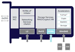
Mellanox is one of the oldest entrants in the SmartNIC space, but it was through acquisition. Its current Bluefield 2 solution (Fig. 2) was built from the purchase of Tilera via EZchip in 2015. Tilera had one of the first highly parallel SmartNIC implementations using intellectual property, which evolved from a much earlier MIT research project.
Essentially, Tilera arranged processing cores as tiles on their chip with each core having a high-speed bus to the four cores around it. Its flagship product back in 2013 supported up to 72 MIPS cores, memory controllers, encryption modules, a PCIe block, and the mPipe, a collection of channels out to several MACs with SFP+ connectors. Mellanox advanced this forward by replacing the cores with Arm and swapping out the mPipe for ConnectX logic. The current core count is eight Arm v8 A72 cores, just like Broadcom, but only clocked at 2.4 GHz. These are arranged as a cluster of four dual-core Arms. Bluefield is currently using the Avago 16-nm process, but like Broadcom, it too should be going to 7 nm this summer and moving from eight to 12 cores.
While this approach is very similar to the Broadcom Stingray, it lacks the parallel P4 processor at the heart of Broadcom’s architecture. P4 is where everyone is going, just not everyone has stated it, or gotten there, yet. Broadcom, Xilinx, and Pensando below are all focused publicly on P4. This again is where Cumulus Networks comes in—it has experience in P4 programming, and it wouldn’t be a surprise for Nvidia to craft a P4 packet processing engine to front end a future Bluefield offering.
Pensando
The newest SmartNIC startup is Pensando, founded by the "MPLS" team of Mario Mazzola (Vice Chairman of the Board), Prem Jain (CEO), Luca Cafiero (Board member & technical advisor), and Soni Jiandani (Chief Business Officer), a team of engineers who spearheaded the development of several of Cisco Systems's key technologies, and founded four startups that were acquired by Cisco. John Chambers—the former CEO of Cisco—is the Chairman of the Board.
Given the reputations of the founding group and Chairman of the Board, and prior experience, the general consensus is that Pensando is proving its technology works with some anchor customers, and then it will be packaged up for a Cisco acquisition. Cisco has some generic NIC technology and several internal SmartNIC projects, but the word on the street is that these may not see the light of day, so Pensando is clearly looking to fill this void.
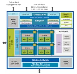
Pensando originally had two products, but recently dropped back to a single one, the DSC-25 Distributed Services Card, which even sounds like a Cisco product name. It appears to be a single P4 processor chip, with an Arm for some auxiliary processing, both of which the datasheet claims support up to 4 GB of onboard memory (Fig. 3).
The processor, called Capri, is a P4 programmable unit with multiple parallel stages; the exact degree of parallel processing is unknown, though, as is the packet performance, latency, and jitter which haven’t yet been published. Pensando keeps the P4 applications tight so that they remain inside Capri’s cache as a cache miss, resulting in a memory fetch for an instruction that kills performance across all metrics. Other additional computational units, called Service Processing Offloads, handle encryption, storage processes, and other tasks. Pensando claims that Capri can provide wire-rate performance.
Netronome
Netronome the is grey-bearded startup in this space, having started in 2003 and taken five rounds of funding thus far for a total of $73 million. The company been actively promoting P4 since 2015, when it demonstrated its first SmartNICs utilizing the technology. Since then, Netronome has made some significant strides, but lately the rumors are that it’s stumbled and may be exiting the market.
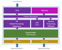
Figure 4 shows Netronome’s current NFP4000 Flow Processor architecture. Instead of a single P4 processing engine, the company leverages two classes of programable cores: 48 packet processing cores, and 60 flow processing cores. Additional silicon is dedicated to classification, modification, and management. All of these cores can be programmed in P4.
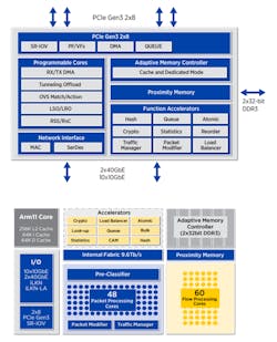
The result is that Netronome claims the cores can sustain a single 100-Gb/p link at wire-rate, 148 million packets per second, with millions of exact matches and wild-card flows. Also, they can support 100K+ tunnel connections requiring encapsulation. An extremely long list of target applications that the technology can support includes intrusion detection systems (IDS), intrusion prevention systems (IPS), next-generation firewall (NGFW), routers, load balancers, packet brokers, SDN, NFV, and a whole host of other applications.
Fungible
One other potentially large snake is still lurking in the P4 grass that has yet to raise its head, namely Fungible. It’s on the verge of announcing a product after having taken three rounds of funding totaling nearly $300M, with $200M of that coming from Softbank Vision in the C-round last year. Currently, the company has 180 people, no products, no revenue, and no visible customers.
Fungible claims to be producing a data processing unit (DPU), but the actual architecture and makeup is unclear. The company provided the diagram shown in Figure 5, which is about as cloudy as an architecture diagram can become before becoming pointless. Various articles have mentioned that its product will be released this summer, so we wanted to make sure this company was on your radar.
One of Fungible’s founders, and the Chief Architect, is formerly a 10-year veteran of Chelsio Communications, which specialized in storage-centric Ethernet NICs. The VP of Software and Firmware Engineering is also a former Chelsio employee, but for 13 years. So, while Chelsio was ASIC-driven in the past, the cost of producing a leading-edge SmartNIC Ethernet controller ASIC from scratch these days would easily consume over $50M of its precious capital.
The speculation is that Fungible will take the path of least resistance to reach revenue and utilize an FPGA platform for its initial product with the secret-sauce ASIC design loaded into this platform. It could then shake out the design while beginning to chase customers and revenue. Loading a design into an FPGA would enable the company to easily fix design flaws and support rapid customer-driven improvements. Today, FPGAs are enormous, and we’ve started seeing full-blown processor architectures like RISC-V being loaded into these platforms.
Intel
When it comes to a chip company, you don’t get any bigger than Intel. For more than a decade, Intel has maintained an unbroken line of high-performance 10-GbE controllers. Its XL710 platform has shipped millions of units and is a staple in many data-center servers.
For the new N3000 SmartNIC, Intel has crafted a board using five of its chips (Fig. 6). This is an expensive approach, as most vendors strive for single-chip designs. Intel fused together a pair of its XL710 Ethernet controllers and an Arria 10 FPGA using a 48-lane PEX8747 PCIe Generation three-switch chip. Eight lanes go to each of the XL710s, 16 lanes to the Arria, and 16 lanes down to the PCIe socket. The fifth chip is a MAX 10 FPGA baseboard management controller (BMC) that manages the FPGA, much like Arm cores are used on other SmartNICs to handle control-plane management.
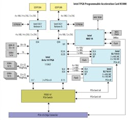
The board has dual QSFP28 ports that go straight to the FPGA. Then eight lanes of 10G leave the FPGA to each XL710. This is a classic bump in the wire approach, and it enables the FPGA to work on packets prior to them being passed to the XL710s.
Building a NIC using an off-the-shelf Ethernet controller and an FPGA is nothing new. Back in 2012, Solarflare Communications placed an FPGA between the two QSFP ports on a NIC and its Ethernet controller to create the Application Onload Engine (AOE) platform. This was a precursor to the N3000 design selected by Intel, but it enabled Solarflare to deliver impressive tick-to-trade results for financial customers, at the time 350 ns. Today, some eight years later, the record is 24.2 ns.
Intel’s approach allows the FPGA to do packet processing prior to the XL710. The company’s FPGA has 1,150K programable logic elements and two banks of 4 GB of DDR4 memory, each giving it ample room to handle SmartNIC tasks like:
- Virtual Broadband Network Gateway (vBNG)
- Hierarchical Quality of Service (HQoS)
- Packet classification, policing, scheduling, and shaping
- Virtualized Evolved Packet Core (vEPC)
- 5G Next-Generation Core Network (NGCN)
- Internet Protocol Security (IPSec)
- Segment routing for IPv6 (SRv6)
- Vector Packet Processing (VPP)
- Virtual Radio Access Network (vRAN)
While Intel has targeted the above workloads for the N3000 platform, it’s unclear at this point if the company delivered all of the necessary software to offload each of these applications on this SmartNIC. SmartNIC consumers will learn that the devil is in the software—all of these companies are excellent at hardware, but software delivery is a whole other discipline.
Xilinx
The other standout FPGA entrant in the SmartNIC space is from Xilinx, the first company to commercialize the FPGA in the mid-1980s. Today, Xilinx stands atop the FPGA hill while Intel is running a distant second. The company acquired Solarflare Communications in the fall of 2019, and Solarflare has been building both ASIC- and FPGA-based NICs for electronic trading since 2012. The Solarflare engineering team out of Cambridge in the U.K. was behind Xilinx’s Alveo U25 SmartNIC (Fig. 7). Hence, it leverages the company’s nearly 10 years of experience in this market.
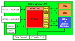
The Alveo U25 attaches the dual SFP28 ports directly to a Zynq series chip. The Zynq is an actual system-on-chip (SoC) as it includes not only an FPGA, but also a quad-core Arm A53 for packet processing. The Zynq then connects directly to the host server via eight lanes of PCIe Gen 3 or through the SerDes to the X2 Ethernet controller chip, which is also connected via eight lanes of PCIe Gen 3 to the host. This approach enables the Zynq to process packets before they’re passed to the X2 chip, or to bypass the X2 entirely.
The Alveo U25 also includes 6GB of DDR4 memory accessible to the Zynq’s FPGA and Arm cores by programs running on this chip. The FPGA has 520K logic elements available, but the provided quad-core Arm more than makes up for the reduced available gate count.
Xilinx is bringing the Alveo U25 to market to initially address customers that have requested Open virtual Switch (OvS) offload capability. The company announced that in the near future, it will be adding offloads for IPsec, machine learning (ML), deep packet inspection (DPI), video transcoding, and analytics. Exhibiting its SmartNIC versatility, two years ago, in the run-up to acquiring Solarflare, the two companies were partners, publicly demonstrating the XtremeScale X2 controller logic running as a soft-NIC inside a much larger FPGA at the OCP Summit.
Like Intel, Xilinx has several computational chip product lines: Kintex, Virtex, Zynq, and Versal. Kintex and Virtex are pure FPGAs, and some models in this line have nearly 3,000K logic cells, almost triple what Intel has used in its N3000. Xilinx has also worked with silicon interposers and layered up to 16 GB of high bandwidth memory (HBM) on Virtex chips. This technology is also appearing in other chips across all four chip lines.
Zynq, which is Xilinx’s SoC chip line, includes FPGA programable logic along with quad-core Arms, real-time Arm cores, DDR controllers, and connectivity logic for both Ethernet and PCI Express. Versal goes way beyond SoC to an adaptive compute acceleration platform (ACAP) built on 7-nm chip technology. The ACAP extends the Zynq architecture by adding hundreds of artificial-intelligence (AI) cores, digital-signal-processing (DSP) engines, and much more. AI cores are somewhat new, but they’re essentially single-precision compute engines. Eventually, the company will couple its publicly demonstrated SoftNIC with Versal.
Current SmartNIC Climate
As we’ve seen from Netronome and even Solarflare Communications, SmartNICs have been a long time in coming. Potentially big customers like Google and Amazon have removed themselves from the market by designing and building their own in-house solutions. Meanwhile Facebook and Microsoft have provided high-level architectures that industry vendors have since rushed in to fill.
While all this was being sorted out, SoCs and more importantly FPGAs have matured to a point where they can now become the foundational technology for SmartNICs. A decade ago, we were awash in GPU products as the first significant wave in hardware-acceleration technology hit. Now with FPGAs scaling above three million logic units, we're also tightly coupling them with other composable processing blocks for networking, memory, storage, and compute. Compute, in this case, means on-chip clusters of cores via SoC blocks or even ACAPs.
With such advances, we're starting to recognize the formation of the second wave of hardware acceleration. Where GPUs needed new programming APIs and tools to support those platforms, the same will be true of FPGAs. The difference, though, is that this technology has been evolving for over 35 years, and its time is coming. So, as the SmartNIC market is finally emerging, it will converge with the next wave of FPGA-based hardware accelerators. That will form a superposition of sorts in the acceleration market, perhaps facilitating a sea change and altering our perspective of computing going forward.
SmartNICs are pushing computation and, therefore, acceleration to the edge of the network, freeing up server CPUs to work on more solutions focused on complex business-critical processing. Studies have shown that networking in highly virtualized environments can consume upwards of 30% of the host's CPU cycles’ processing tasks like OvS transactions.
Imagine if storage functions, encryption, DPI, and sophisticated routing could be done in a SmartNIC? This could potentially deliver back to the host CPU complex a significant portion of the CPU cycles usually spent processing these workloads.
To stay ahead of the big guys, new companies like Pensando and Fungible will continue to breathe innovative features and capabilities into the SmartNIC market. At the same time, technology leaders like Xilinx, Intel, Broadcom, and Nvidia will improve foundational computing cores and specialized P4 processing engines. Exciting times are ahead.
Scott Schweitzer is Technology Evangelist at Xilinx.
Read mores articles from the Communication and System Design Series: Have SmartNIC - Will Compute
About the Author

Scott Schweitzer
Director of SmartNIC Product Planning, Achronix Semiconductor
Since his baptism on the altar of the TRS-80, Scott has been a lifelong technology evangelist. He's written profitable software products, built hardware, and formally managed programs for IBM, NEC, Solarflare, and now Xilinx.
After two decades plugging along with single socket computing platforms, Scott joined NEC in 2003 to manage its new Intel Itanium multi-core 64-bit Super Computing Server, and he's never looked back. In 2005, Scott shifted his focus to clustering for Super Computing and extreme performance networking.
As 10-GbE adoption ramped up, he launched his wildly popular 10GbE.net blog. With market changes in 2017, Scott rolled 10GbE.net into the Technology Evangelist, a blog with thousands of monthly page views, and an accompanying podcast.
Comment About the Article
To join the conversation, and become an exclusive member of Electronic Design, create an account today!

Leaders relevant to this article: