SiP—Leveraging Mass Production on a Small Scale
>> Electronic Design Resources
.. >> Library: Article Series
.. .. >> Series: Path to Systems
System-in-package (SiP) technology is at the beginning of its revolution. Some see the SiP in the same way as a system on chip (SoC)—as an IC component with no simple path to further customization. Also, the economics of scale relegate the device to a high-volume manufacturing process in addition to the long design cycle time. Which isn’t an issue if you, as a systems engineer, need millions of devices per year. However, new innovators and entrepreneurs are left out.
So, is there a way that systems designers can take advantage of the SiP technology to further integrate without the need for a high-volume application? Apparently so, as capabilities loom on the horizon that allow for more integration with less volume using SiP.
SiP Design and Manufacture Today
There are compelling reasons for a SiP to be the solution to systems integration. We detailed several, including simplification, miniaturization, cost reduction, and reliability in Part 2 of this series. In fact, the same requirements that drove the SoC development are likely to drive the SiP roadmap as well. However, SiP capability will be able to bypass many of the limitations presented by SoC without sacrificing much of the system integration achievable through an SoC.
For example, Figure 1 shows a block diagram of a SiP1with a variety of functional blocks. This example is an embedded system that has different IP blocks, with several different semiconductor process nodes. In addition, functional blocks make integration of the SiP into the system easy. Some of these subsystems, such as the parallel and serial interfaces, are integrated into the SoC, while other subsystems like the DDR memory and power-management IC are independent components integrated into the SiP. This allows the SiP to be a functional system-level block rather than a design challenge, which has become the case with current SoCs.
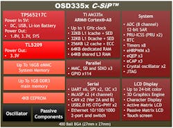
1. OSD335x C-SiP system-in-package block diagram.
The Figure 1 block diagram definition is the result of the initial stages of the SiP’s design. An important decision to make here is which components go in the SiP and which do not. Design complexity, functional importance, and package/die size are some of the factors that influence this decision. Once the device is well defined in the block diagram stage, computer-aided design (CAD) tools are used to actualize the SiP device. SiP and IC manufacturers often have specific design rules that may not be common or industry standard. So, it’s important to work with the manufacturer during the design stage. When the design is complete, the release package is sent to the manufacturer.
An example process flow of SiP manufacturing process is shown in Figure 2. Ideally, all active components in the SiP are in die form, but they can also be packaged parts. The manufacturing process might vary based on the integration techniques and the target size/specification to be achieved. The process described in Figure 2 illustrates a simple surface-mount device (SMD) attach process for surface-mount components and wire bonding for die integration.
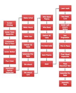
2. High-level manufacturing flow of a SiP.
The SMD components of the SiP are attached to a substrate. This substrate is a printed circuit board built with micron-level design rules that allow for a miniaturized circuit board, tight integration, and better bandwidth and power performance. After the assembly goes through a reflow, it’s pre-baked for die attach. After the die attach has cured, the dies are then attached and wire bonding is performed. This assembly is baked yet again and molded with a preselected mold compound that’s suitable for the system. After the mold compound is set, the package goes through solder-ball attach and dry bake. Several quality checkpoints are embedded in the process to enable process specific fault detection.
Overcoming the Challenges of the Current Design and Manufacturing Process
As described in Part 2, this new SiP technology presents new challenges. Some challenges, such as lack of flexibility and inability to customize, are technical. Other challenges, like the need to be high volume to be viable in the IC manufacturing process, are economic. While there’s a desire to integrate more functional blocks into the system, doing so compromises system flexibility. The greater the number of functional blocks, the less flexible the SiP becomes, which means lower volume, application specific and higher cost, making integration nonviable.
Although not as complex as with an SoC design, making changes to a system component in the SiP still provides a significant hurdle. Moreover, users desire customizability to have better control of their own design as well as make choices of the functionality of the SiP. All of this, while possible, has cost and time burdens associated with it. The good news is, there are solutions that can overcome these challenges with minimum effort spent in time and money.
Semi-Custom SIP Devices
Semiconductor manufacturers have developed many solutions over the years that enable higher integration and better manufacturability for SiPs. Flip-chip, 3D die stacking, and package on package (PoP) are examples, essentially adding the z-axis to the integration environment. The flexibility of bond-wire placement and specialized mechanical tools have played an important part in these solutions.
These solutions, however, are either highly integrated and don’t match a lot of system requirements or remain too risky to be integrated into the production flow to be considered as effective enablersThe only way to maintain the scalability of the manufacturing process while delivering more integration and functionality is through customizability, which is transparent to the manufacturing process. By making it transparent, the advances in manufacturing processes and adapting the SiP design process to lend itself to customization can be an ideal solution.
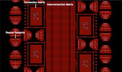
For example, Figure 3 shows a version of a customizable part (connection matrix) of a substrate.2 The central pad (25) is where a die would attach to the substrate and bond wires would be used to connect the die pads to appropriate substrate pads as needed. The central pad can accommodate different-sized dies. This layout can be used to make a configurable SiP by programming the pick-and-place machine and the wire-bonding machine appropriately.
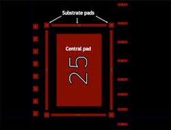
3. Customizable die footprint.
This is only one, rather simple, example of how configurable design choices can lead to customizable SiPs. Another example, or rather an extension to this die-attach configuration, is a configurable substrate layout that allows for connecting signals between multiple dies. Figure 4 shows a customizable interconnection matrix that can be used to create a configurable SiP system. Signals from the die components in Figure 3 as well as other passive/active components can be connected to a connection matrix shown in Figure 4 by signal traces on the substrate. Then they’re electrically connected to other signals with bond wires on the connection matrix. In a sense, this makes the connection matrix, when combined with the die-attach pads, a miniature breadboard.

4. Customizable interconnection matrix.
This combination of the central connection matrix and the interconnection matrix has several applications; for example, signal conditioning. The interconnection matrix with a number of connection matrices and passive components connecting into the interconnection matrix placed around it on the substrate (Fig. 5) can allow for a large number of op-amp-based signal-conditioning systems.

5. Customizable substrate design.
As mentioned, this is one of many ways to create a customizable substrate. The takeaway here is that customizability is a design methodology that increases flexibility and enables low-volume innovators while providing access to the latest and greatest integration methods.
So, the next question is, “How can the design of a SiP be done to build configurable SiPs?” Based on the application, there are many answers to this question. While the above example is suited for signal conditioning, similar design methodology can be implemented for other areas of computing and embedded design.
What Are the Issues?
The configurable SiP creates a new set of challenges. For example, new software tools that enable this design methodology are necessary. Challenges on the manufacturing side include programming the capability in the pick-and-place/bond-wiring machines such that a production line delivers different customizations of a configurable SiP while the line remains the same.
Conclusion
The customizable SiP solution, as it progresses and morphs into new SiP designs, represents a new paradigm in semiconductor manufacturing. The end goal of this technology is to provide a SiP to the system designer who has a need for low-volume run rates with the cost associated with a high-volume run rate.
Is there a system that allows individuals to input their designs while delivering SiP’ed packages without the drawbacks of the low-volume manufacturing cost as well as complex design effort? Such a design methodology reduces time and money spent on the design while providing a path to integration beyond standard components on a PCB. We believe the answer is yes.
- Series: Path to Systems
- Prior article in this Series ... Why a SiP?
- Next article in this Series ... A SiP of Reliable Advantage—Systems Under Test
References:
1. https://octavosystems.com/octavo_products/osd335x-c-sip/
2. https://patents.google.com/patent/WO2017040967A1/en?oq=WO2017040967

About the Author
Neeraj Dantu
Applications and Systems Engineer
Neeraj Dantu is an Applications and Systems Engineer at Octavo Systems. As a recent graduate, Neeraj is excited to be a part of Octavo’s highly experienced team. He also looks forward to help Octavo change the face of electronic design and manufacturing. With diverse research experience in hardware design, machine learning, computer vision, and signal processing, Neeraj brings a fresh perspective to the team. Neeraj earned his B.Tech (Bachelor of Technology) in Electronics and Communications Engineering from The LNM Institute of Information Technology, India, and a Masters in Electrical Engineering from Rice University.
Gene Frantz
Chief Technology Officer
Masood Murtuza
Co-founder and Manager of Package Engineering
Masood Murtuza is the Manager of Package Engineering and a founder of Octavo Systems. Prior to joining Octavo, Masood was a Fellow at Texas Instruments, where he held various leadership roles in the Packaging and Assembly Process Engineering teams. During his tenure at TI, he introduced a number of new semiconductor packaging technologies. He also helped advance innovation in technology development across the company by establishing new methodologies in package and assembly development process. Masood holds 25 patents and has authored or co-authored over 15 papers. He received his BTech in Mechanical Engineering from the Indian Institute of Technology, Madras, India, and an MSc in Naval Architecture from University College, University of London.
Gene Frantz
Chief Technology Officer
Gene Frantz is one of the founders and the visionary behind Octavo Systems. He currently serves as Chief Technology Officer. He is also a Professor in the Practice at Rice University in the Electrical and Computer Engineering Department. Previously, Gene was the Principal Technology Fellow at Texas Instruments, where he built a career finding new opportunities and building new businesses to leverage TI’s DSP technology. Through this work he became highly regarded in the industry as a leader in DSP technology. Gene holds 48 patents, has written over 100 papers/articles, and presents at conferences around the globe. He has a BSEE from the University of Central Florida, a MSEE from Southern Methodist University, and a MBA from Texas Tech University. He is also a Fellow of the IEEE.
Comment About the Article
To join the conversation, and become an exclusive member of Electronic Design, create an account today!

Leaders relevant to this article: