What’s in Storage at the Flash Memory Summit?

The Flash Memory Summit is coming to the Santa Clara Convention Center in August. I will be there hosting a pair of sessions on embedded flash-memory technology (Embedded Applications Part 1 and Part 2). These will include a number of topics like “Improving Lifetime Estimates for Embedded Flash” from Tom McCormick, Chief Engineer/Technologist at Swissbit and “Choosing the Right Flash Technology for Embedded and Industrial Applications” with C.C. Wu, VP Embedded Flash at Innodisk.
Processors still take a back seat to the insatiable demand for storage and the seemingly daily raising of both performance and capacity bars. Quite a few of the latest announcements will occur during the Flash Memory Summit, and most of the latest technology will be on display.
Some recent flash storage announcements include Toshiba’s 3D flash memory (Fig. 1), which utilizes through-silicon-via (TSV) technology in a 48-layer die. The BiCS FLASH also uses 3-bit-per-cell (triple-level cell, TLC) technology to deliver a 1-TB chip in a 13- by 18-mm VGA package. The die are stacked 16 layers high and have an interface speed of 1066 Mb/s.
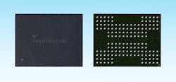
1. Toshiba’s 3D flash memory employs through-silicon-via (TSV) technology.
Questions continue to swirl around flash, which Electronic Design has addressed with articles like "11 Myths About NAND Flash." And we’ve covered changes like putting flash memory directly on the memory channel with Diablo Technologies’ Memory 1.
Flash will not be the lone technology on the summit floor, though. Also on display will be innovations from the likes of Everspin, with its Spin-Torque MRAM (ST-MRAM), and Kingston Technology, with its KC1000 NVMe PCIe SSD (Fig. 2).
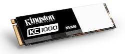
2. Kingston Technology’s KC1000 NVMe PCIe SSD packs up to 960 GB of MLC flash storage into an M.2 module.
Of course, Samsung will be there with its 64-layer, 256-Gb V-NAND flash chips and modules (Fig. 3). The TLC storage features a 1-Gb/s transfer rate; meanwhile, V-NAND has only a 500-µs programming time. The cells employ a charge-trap-flash (CTF) approach.
One presentation that looks very interesting centers around NOVA, a file system for Hybrid Volatile/Non-volatile main memories. This could use storage like Memory 1 as well as other non-volatile memory that targets the memory channel like Intel’s Optane.
Some of the newer trends Electronic Design will be covering include topics present at this year’s summit, such as NVMe over Fabrics (NVMf or NVMeF) that include Ethernet and InfiniBand. This is designed to scale to high-end systems with thousands of nodes. It leverages technologies like RDMA over Converged Ethernet (RoCE).
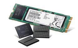
3. Samsung’s M.2 module uses its latest 64-layer, 256Gb V-NAND flash chips.
So, as the Flash Memory Summit’s Lance Leventhal has said to me “Come see a real-life fossil, an actual editor for a print magazine. It's like seeing the last man to drive a horse-drawn streetcar or the last person to star on a radio show. Don't miss this once-in-a-lifetime opportunity to see history in the flesh.” It seems that technology editors are a rarity these days.
Hope to see you there. If not, check back later on my coverage from the show.

About the Author

William G. Wong
Senior Content Director - Electronic Design and Microwaves & RF
I am Editor of Electronic Design focusing on embedded, software, and systems. As Senior Content Director, I also manage Microwaves & RF and I work with a great team of editors to provide engineers, programmers, developers and technical managers with interesting and useful articles and videos on a regular basis. Check out our free newsletters to see the latest content.
You can send press releases for new products for possible coverage on the website. I am also interested in receiving contributed articles for publishing on our website. Use our template and send to me along with a signed release form.
Check out my blog, AltEmbedded on Electronic Design, as well as his latest articles on this site that are listed below.
You can visit my social media via these links:
- AltEmbedded on Electronic Design
- Bill Wong on Facebook
- @AltEmbedded on Twitter
- Bill Wong on LinkedIn
I earned a Bachelor of Electrical Engineering at the Georgia Institute of Technology and a Masters in Computer Science from Rutgers University. I still do a bit of programming using everything from C and C++ to Rust and Ada/SPARK. I do a bit of PHP programming for Drupal websites. I have posted a few Drupal modules.
I still get a hand on software and electronic hardware. Some of this can be found on our Kit Close-Up video series. You can also see me on many of our TechXchange Talk videos. I am interested in a range of projects from robotics to artificial intelligence.
Comment About the Article
To join the conversation, and become an exclusive member of Electronic Design, create an account today!

Leaders relevant to this article: