Members can download this article in PDF format.
What you'll learn:
- Advances in EV technology to make them more practical.
- How SiC MOSFETs will help meet the current challenges in the EV arena.
- The all-important high switching speeds of SiC MOSFETs.
Silicon-carbide (SiC) power FETs are finding increased application in the bridge inverters of modern electric vehicles (EVs) as automakers struggle to satisfy the growing demand for products that offer range, performance, and a sticker price equivalent to their fossil-fueled counterparts (Fig. 1). But, along with their high efficiency and excellent performance, SiC FETs bring new requirements and design challenges.
This article provides an overview of the role that SiC devices are playing in the next generation of traction inverters, and what it takes to accommodate their unique characteristics.
New Realities for EVs
Although the EVs we will be buying in 2025 won't look much different than those that entered the market around 2018-2020, their resemblance will be only skin deep. All forms of electric transportation are undergoing a period of rapid evolution as a combination of market forces and technical innovations are making them more practical and more affordable. These include:
Higher operating voltages
While nearly all of the batteries and power-conversion systems in today's EV operate at 400 V, most next-gen EVs will operate at 800 V and, in some cases, even higher voltages. Doubling the operating voltage cuts the current flowing through the EV's wiring harness by roughly 50%, which, in turn reduces its weight and cost. Equally important, the higher voltage can dramatically shorten battery-charging times while reducing losses due to resistance heating.
Although some silicon IGBTs can operate at these elevated voltages, they must be fabricated with larger geometries that subject them to higher losses and makes it difficult to switch efficiently at the higher frequencies required to drive many modern motors. In contrast, SiC's inherent electrical properties allow them to be rated for 1200-V operation (typically required for use in an 800-V EV powertrain) while still delivering the low losses and high operating frequencies required for tomorrow’s EVs.1
Higher power densities
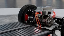
Designers are working hard to reduce the size of high-power electronic subsystems, such as traction inverters and onboard chargers (OBCs) as both a cost-saving measure and to maximize the vehicle's usable space. When applied to bridge inverters, using smaller, cooler-running drive modules allows designers to place them closer to their point of load (PoL), often co-located with the motor/transaxle assembly (Fig. 2).
Two of the most common techniques for increasing power density are to use more efficient power devices (such as SiC or GaN), and incorporate more highly integrated components into the design. Reducing the waste heat generated by a high-power assembly can cut the size of the heatsink and other cooling components by 90% or more. In addition, it replaces discrete components in the driver and protection subsystems with integrated solutions that require much less PCB real estate to implement.
Lower solution costs
EVs are becoming increasingly popular, despite the fact that they cost significantly more than an equivalent ICE-powered vehicle. But for EVs to eventually displace their carbon-fueled counterparts, automakers must narrow or eliminate that price gap.
Some of these savings will be realized by the economies of scale due to increased production and next-gen batteries that are expected to cost significantly less per kilowatt-hour. Nevertheless, SiC will play an important role in creating traction inverters (and other high-power subsystems) that enable the use of smaller, lighter wiring harnesses, require less cooling, and can use smaller batteries to deliver the same range.
SiC Solutions
SiC MOSFETs will play an important role in meeting these challenges, in large part because they have a lower reverse-recovery charge (Qrr) and their on-resistance (RDS(on)) is more stable over-temperature, suiting them for operating at higher switching speeds. As a result, they can turn more of an EV's stored capacity input into usable motor output than IGBTs. And as we learned, they’re smaller than IGBTs and run cooler, further reducing weight, size, and energy waste in an electric drivetrain.
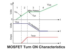
But for all their advantages, SiC devices also possess a unique set of electrical properties that require them to be treated very differently than the IGBTs they replace. To begin with, SiC switching devices are more susceptible to damage from short circuits than IGBT technology. As a result, care must be taken to minimize the switching and conduction losses they experience, including their turn-on and turn-off energy. This is most evident in the SiC device's gate-charge characteristic, which includes a flat, horizontal section called the Miller plateau (Fig. 3).2
When a SiC MOSFET switches, its gate-to-source voltage (VGS) becomes clamped at the Miller plateau voltage (Vplt) due to gate capacitance. It remains at this threshold (VGSTH) until the gate's charge is overcome. The more time a MOSFET spends between the on and off states, the more power is lost, and the greater potential for damage to occur to the device.
Accelerating the MOSFET's transition through the Miller plateau requires its gate to be driven with enough current to quickly add or remove the unwanted gate charge. The equation below is used to calculate the charge that the isolated gate driver will need to add or remove to the SiC MOSFET's gate before accomplishing a full state transition. As shown by this simple equation, the MOSFET's gate current is proportional to the gate charge:
QGATE = IGATE × tSW
where IGATE is the isolated gate-driver IC current and tSW is the MOSFET's turn-on time.
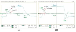
It's easy to infer from this equation that the MOSFET's switching losses and self-heating can be reduced by increasing its gate-drive current to shrink the time it spends in the Miller plateau. In addition, higher gate currents also produce a sharper transition between states (Fig. 4).
High-Speed Waveforms
These fast transitions also are necessary to produce the fast-switching waveforms needed to drive the advanced electrical motors used by many EVs, which run at speeds as high as 20,000 RPM. In high-power traction-inverter applications (≥ 150 kW), SiC switches require large gate-driver currents (typically 10 to 30 A) to produce the slew rates that minimize losses and support high multi-kilohertz switching speeds.
While these high-speed drive waveforms offer many advantages, the rapid transitions also produce voltage overshoot and electromagnetic interference (EMI) in the form of conducted ground currents. These currents may cause the inverters' control circuitry to malfunction. Moreover, the motor itself can suffer from high dv/dt given the potential for short circuits in the capacitance between the windings.
No single approach can completely address these issues. However, using a "smart" gate driver that can adjust its gate current to accommodate changing switching speeds under varying conditions, such as temperature, load, and voltage, is a good place to start. A gate driver that's optimized for driving SiC devices also should include a fast shutdown function that protects the FET against damage from short-circuit conditions.
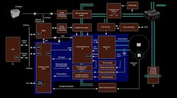
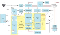
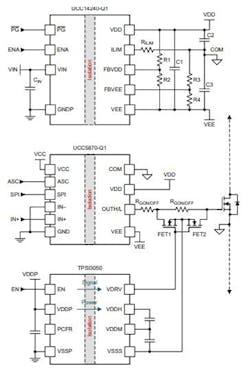
Using gate resistance to control the gate driver’s output source and sink current helps optimize the tradeoff between dv/dt and power losses. Figure 5 shows an implementation of a gate driver with an adjustable output drive strength that can optimize its companion SiC MOSFET's slew rates to accommodate variations in temperature and current requirements. In addition to protecting the inverter against adverse conditions, reducing EMI, carefully controlled drive current can further reduce losses, thereby extending driving range.
References
1. “HEV/EV Traction Inverter Design Guide Using Isolated IGBT and SiC Gate Drivers,” Audrey Dearien, Texas Instruments, June 2020 – Revised October 2022.
2. “Design Priorities in EV Traction Inverter with Optimum Performance,” Xun Gong, Texas Instruments – September 2022.
3. “Traction Inverters – A Driving Force Behind Vehicle Electrification,” Waqar Mehmood, Audrey Dearien, VC Kumar, and Krunal Maniar, Texas Instruments.
