Power Management Chapter 14: Circuit Protection Devices

This articles is part of the Power Management Series in the Power Management section of our Series Library.
Download this article as a .PDF eBook.
Several types of devices are employed in electronic systems to protect against voltage transients, power surges, and excessive voltage or current. Varistors is one of those devices that protect against excessive transient voltages by shunting the current created by the excessive voltage away from sensitive components.
A varistor’s resistance varies with the applied voltage. It has a nonlinear, non-ohmic current–voltage characteristic similar to a diode, except that it has the same characteristic for both directions of traversing current. At low voltage it has a high electrical resistance that decreases as the voltage is raised. The most common type of varistor is the metal-oxide varistor (MOV). It is electrically equivalent to a network of back-to-back diode pairs, each pair in parallel with many other pairs.
When a small or moderate voltage is applied across an MOV’s electrodes, only a tiny current flows, caused by reverse leakage through the diode junctions. When a large voltage is applied, the diode junction breaks down due to a combination of thermionic emission and electron tunneling, and a large current flows. The result of this behavior is a highly nonlinear current-voltage characteristic, in which the MOV has a high resistance at low voltages and a low resistance at high voltages.
A varistor remains non-conductive as a shunt-mode device during normal operation when the voltage across it remains well below its “clamping voltage”, thus varistors are typically used for suppressing line voltage surges.
Varistors will eventually fail from not successfully limiting a very large surge from an event like a lightning strike, where the energy involved is many orders of magnitude greater than the varistor can handle. Follow-through current resulting from a strike may melt, burn, or even vaporize the varistor. This thermal runaway leads to the failure of dominant current paths under thermal stress when the energy in a transient pulse exceeds the manufacture’s “Absolute Maximum Ratings”. You can reduce the probability of catastrophic failure by increasing the rating, either by using a single varistor of higher rating or by connecting more devices in parallel.
MOV
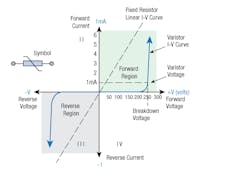
The most common type of varistor is the metal-oxide varistor (MOV) that contains a ceramic mass of zinc oxide grains, in a matrix of other metal oxides sandwiched between two electrodes). The boundary between each grain and its neighbor forms a diode-like junction, which allows current to flow in only one direction. When a small or moderate voltage is applied across the electrodes, only a tiny current flows, caused by reverse leakage through the diode junctions. When a large voltage is applied, the diode junction breaks down due to a combination of thermionic emission and electron tunneling, and a large current flows. The result of this behavior is a highly nonlinear current-voltage characteristic, in which the MOV has a high resistance at low voltages and a low resistance at high voltages. Fig. 14-1 shows the current vs. voltage of a typical MOV compared with an SiC diode.
(1)
Where:
Pout_max = Maximum output power of the dc-dc converter
Vin_min = Minimum input voltage on the input pins of the dc-dc converter
E = Efficiency of the device at Pout_max and Vin_min
To prevent damage to device components, select a fuse current rating with a large enough current capability so that the fuse will not open under steady state conditions, yet will open during an abnormal (excessive) overload or short-circuit condition. Therefore, select a fuse to be 150% to 200% percent of the maximum steady state input current at maximum load and minimum line input voltage.
Interrupting rating is the maximum current at rated voltage the fuse can safely interrupt. This rating must exceed the maximum fault (short-circuit) current the circuit can produce. Interrupting ratings for ac and DC currents are different and the fuse data sheet should be consulted before selection.
Temperature derating is the ambient temperature exceeding the standard 23°C. The fuse current rating should be derated (a higher current rating with higher temperatures). Conversely, operating at an ambient temperature lower than the 23°C standard allows use of a lower current rating.
Fuse rating is determined by:

(2)
Where:
I input_max = the current determined from Equation 1 or the device datasheet
Ktemp = the temperature derating factor determined from the derating factor (Fig. 14-2)
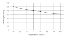
14-2. Fuse derating curves.
The lowest suitable fuse rating is obtained by rounding up the calculated value to the next higher current rating shown in the fuse datasheet.
Melting integral, termed melting I2t, is the thermal energy required to melt a specific fuse element. The fuse element construction, materials and cross sectional area determine this value.
Peak inrush current is usually greater than the steady state current. Also, periodic inrush currents can be sufficiently powerful to warm the fuse element. Though not large enough to melt the element, it can still cause thermal stress to the element. Cyclical expansions and contractions of the fuse element can lead to mechanical fatigue and premature failure.
Calculate the melting I2t values of the fuse for the condition where the product of the peak current squared and the time when the peak occurs is maximum. For example, the steady state current is maximum at low line so a transient load surge needs to be added to the low line current to establish the maximum peak current for an operating condition. But the inrush current is usually maximum at the highest input voltage. The fuse’s melting I2t must be evaluated at the condition with the highest calculated I2t to ensure that the fuse will not open during these “normal” operating conditions.
Select a fuse with the minimum I2t greater than the energy of the inrush current pulse. This ensures that the fuse will not cause a nuisance opening during transient conditions. For reliable system operation for the required number of turn-on cycles, meet the following condition:
I2t Fuse ≥ I2t Pulse × FP (3)
Where:
I2t Pulse = Energy of a current pulse
I2t Fuse = Melting integral of a fuse
FP = Pulse factor (dependent on fuse element construction)
I2t Fuse can be found in fuse datasheets. Do not use the fuse’s maximum melting integral in Equation 3, and use either the minimum or nominal melting integral of the fuse.
Other selection considerations include start-up (inrush) currents and transient load conditions. When a device is initially powered, the input bulk capacitors must be charged. For example, current flowing into the input terminals of a dc-dc converter is approximately I = V/R for typical power supplies with charge times less than 10 mS. When V is the input voltage change, and R is a combination of wiring resistance, your source’s resistance under start-up, and the Equivalent Series Resistance (ESR) of the converter’s input bulk capacitors.
Larger devices often use a large capacitor with very low ESR inside the converter. This inrush current can have a significant effect on the fuse’s life. Size the fuse properly to allow these inrush current pulses to pass without nuisance openings or degrading the fuse element as discussed in melting integral.
To calculate current pulse energy, first determine the magnitude and duration of the current pulse. The most accurate way to determine parameters of a current pulse is to measure this current in the application under minimum and maximum voltage conditions.
TVS
A transient voltage suppressor (TVS) reacts to sudden or momentary overvoltage conditions. One such common device used for this purpose is known as the transient voltage suppression diode that is simply a Zener diode designed to protect electronics device against overvoltage.
The characteristic of a TVS requires that it respond to overvoltages faster than other common overvoltage protection components such as varistors or gas discharge tubes. This makes TVS devices or components useful for protection against very fast and often damaging voltage spikes. These fast overvoltage spikes are present on all distribution networks and can be caused by either internal or external events, such as lightning or motor arcing.
Applications of transient voltage suppression diodes are used for unidirectional or bidirectional electrostatic discharge protection of transmission or data lines in electronic circuits. The level of energy in a transient overvoltage can be equated to energy measured in joules or related to electric current when devices are rated for various applications. These bursts of overvoltage can be measured with specialized electronic meters that can show power disturbances of thousands of volts amplitude that last for a few microseconds or less.
Semtech’s µClamp 3321ZA is a high-performance transient voltage suppression (TVS) for protecting low voltage interfaces (Fig. 14-3). The single-line µClamp3321ZA offers a unique combination of features that protect increasingly sensitive interfaces.
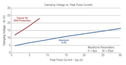
14-3. μClamp3321ZA clamping voltage vs. peak pulse current (tp = 8/20µS).
The µClamp3321ZA delivers optimal transient protection for safeguarding devices operating at 3.3V. It features low dynamic resistance, which provides fast response to transients, as well as low-clamping voltage to protect devices from damage. It is housed in an ultra-small, fully encapsulated package, which provides a more robust solution than conventional CSP (Chip Scale Package) solutions. In addition, the µClamp3321ZA extends the battery life of end-user applications by providing low reverse leakage current of <1nA (typical).
These TVS diodes protect sensitive electronics from damage or latch-up due to ESD. They replace 0201 size multilayer varistors (MLVs) in portable applications such as cell phones, notebook computers, and other portable electronics. They feature large cross-sectional area junctions for con¬ducting high transient currents. This device offers desir-able characteristics for board level protection including fast response time, low operating and clamping voltage, and no device degradation.
It features extremely good ESD protec¬tion characteristics highlighted by low typical dynamic resistance of 0.33 Ω, low peak ESD clamping volt¬age, and high ESD withstand voltage (±15kV contact per IEC 61000-4-2). Low maximum capacitance (5pF at VR=0V) minimizes loading on sensitive circuits. Each device will protect one data line operating at 3.3 V.
μClamp3321ZA is in a 2-pin SLP0603P2X3F package. It measures 0.6 × 0.3 mm with a nominal height of only 0.25mm. Leads are finished with NiAu. The small pack¬age provides flexibility to protect single lines in applications where arrays are not practical. The combination of small size and high ESD surge capability makes them ideal for use in portable applications such as cellular phones, digital cameras, and tablet PCs. Fig. 14-3 shows clamping voltage vs. peak pulse current (tp = 8/20µS).
Among its features:
•
Transient protection for high-speed signal lines: IEC 61000-4-2 (ESD) ±17kV (air), ±15kV (contact)
•
3.3V working-voltage protection for low-voltage interfaces
• Low ESD clamping voltage of 10.5V at 8kV
•
Ultra-small package size: 0.6mm × 0.3mm with nominal height of only 0.25mm
• Low typical dynamic resistance: 0.33 W
• Pb Free and RoHS/WEEE compliant
GDT
A new gas discharge tube (GDT) from Bourns provides a breakthrough flat package design with a volume and space-saving circuit protection design. The two-electrode Model 2017 Series FLAT GDT has a flat package and horizontal circuitry design that meets the need for more sensitive overvoltage protection requirements in high density and space-restricted applications (Fig. 14-4).

14-4. FLAT GDT has a flat package and horizontal circuitry design that meets the need for more sensitive overvoltage protection requirements in high-density and space-restricted applications.
This new series delivers a 75% savings in volume compared to a standard 8 mm Bourns GDT. Typical applications for the new GDT include:
• Telecom CPE
• Industrial communications
• Surge protective devices
• High-density PCB assemblies
The FLAT GDT is consistent with electronic systems that continue to require higher density and performance in smaller packages. However, as designs become increasing smaller, they are more susceptible to damage from transients such as lightning and high voltage surges. Therefore, circuit-protection technology must follow with smaller, more robust devices. GDTs are a popular circuit-protection solution because of their low capacitance, low leakage characteristics, and high surge-current handling capability.
Traditional high current GDTs are cylindrically shaped devices in an 8 × 6 mm size. These dimensions are critical to effectively handling surge energy and maintain electrical isolation. Their diameter and thermal mass provide much of the current handling capabilities for the GDT. Unfortunately, the larger conventional GDTs offer reliable overvoltage protection, at the cost of valuable PCB space.
Besides reducing height and overall volume, Bourns’ new FLAT GDT technology is able to maintain the device’s robust isolation and current-handling overvoltage protection capabilities. This new compact GDT offers superior surge current ratings, low leakage, and insertion loss with constant capacitance regardless of voltage. These devices also do not impact signal or system operation due to their voltage limiting capabilities optimized for long-term reliability and performance to satisfy the needs of today’s more complex electronics equipment.
The FLAT GDT design is patterned after a high voltage insulator, as shown in Fig. 14-5. Similarly, the new GDT design employs “wrinkled” insulating pathways while maintaining the internal gap of the GDT. This allows the GDT to be compressed in the axial direction, reducing its overall volume/size.
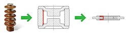
14-5. FLAT GDT design is patterned after a high-voltage insulator, employing “wrinkled” insulating pathways.
The Model 2017 Series is an ITU K.12 Class III GDT device rated at 10 kA on an 8/2μs waveform. The series features DC breakdown voltages ranging from 90 to 500 V. Maximizing its design flexibility, the FLAT GDT offers multiple mounting options including bottom-side PCB, and is available in horizontal and vertical surface mount versions as well as a leadless design for cartridge or clamp fit applications. The Model 2017 FLAT GDT is RoHS compliant.
Fig. 14-6 shows the voltage vs. time plot for the GDT.
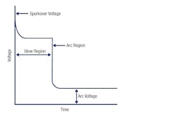
14-6. Voltage vs. time plot for the FLAT GDT.
Read more articles from the Power Management Series in the Power Management section of our Series Library.

About the Author

Sam Davis
Sam Davis was the editor-in-chief of Power Electronics Technology magazine and website that is now part of Electronic Design. He has 18 years experience in electronic engineering design and management, six years in public relations and 25 years as a trade press editor. He holds a BSEE from Case-Western Reserve University, and did graduate work at the same school and UCLA. Sam was the editor for PCIM, the predecessor to Power Electronics Technology, from 1984 to 2004. His engineering experience includes circuit and system design for Litton Systems, Bunker-Ramo, Rocketdyne, and Clevite Corporation.. Design tasks included analog circuits, display systems, power supplies, underwater ordnance systems, and test systems. He also served as a program manager for a Litton Systems Navy program.
Sam is the author of Computer Data Displays, a book published by Prentice-Hall in the U.S. and Japan in 1969. He is also a recipient of the Jesse Neal Award for trade press editorial excellence, and has one patent for naval ship construction that simplifies electronic system integration.
You can also check out his Power Electronics blog.
Comment About the Article
To join the conversation, and become an exclusive member of Electronic Design, create an account today!

Leaders relevant to this article: