With a global market for mobile chargers forecast to reach $25 billion by 2022,1 suppliers of mobile device power adapters and chargers are under pressure to deliver reliable power supply and fast charger capability in compact form factors. While the wide adoption of “standard” adapters utilizing the USB interface, including USB-PD (Power Delivery) devices, helps to improve the end-user experience, it increases the challenge for suppliers to bring products to market that satisfy customer requirements.
Infineon evaluated power-conversion topologies for mobile-device adapters and chargers to determine optimal design, and then compared the performance of an adapter using two types of power semiconductors: superjunction MOSFETs and gallium-nitride (GaN) HEMTs.
Target Topology
The design target was a 65-W USB-PD adapter with a power density of at least 20 W/in.³ to achieve a compact form factor suitable to operation with a broad variety of mobile devices and operating efficiency greater than 90%. Because the design needs to recover energy from leakage inductance and provide zero voltage switching (ZVS) in most or all operating conditions, most of the single-ended topology choices can be ruled out.
In the evaluation, Infineon considered five half-bridge switched-mode power-supply (SMPS) topologies:
- PFC flyback with secondary-side power pulsation buffer
- Flyback converter with a fixed (high) output voltage and subsequent buck converter
- Flyback converter with wide output voltage range
- Cascaded asymmetrical PWM flyback converter (with primary side of two cascaded half-bridges)
- Asymmetrical (hybrid) PWM flyback converter
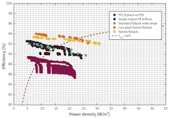
Figure 1 shows the results of optimization studies for full load operation at worst-case input voltage (Vin = 90 V) and highest output current (Iout = 4 A). The figure also shows a thermal limit line (red), which defines the minimum efficiency required to allow passive dissipation to keep the surface temperature of the adapter below 70°C at a given power density.
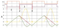
Figure 2 depicts the asymmetrical PWM flyback with synchronous rectification circuit, which was determined to be the optimal topology. High conversion efficiency is achieved with ZVS of the primary-side half bridge by utilizing the magnetization current and zero current switching (ZCS) of the synchronous rectification switch. It operates with a fixed on-time of the low-side switch of the primary half-bridge, which is determined by the resonance frequency, as well as a varying on-time of the high-side switch, which depends on output voltage and thus results in varying switching frequency.
A prototype USB-PD adapter employing 500-V/140-mΩ superjunction MOSFETs was developed to further evaluate the design. It supports output-voltage profiles ranging from 5 V/3 A to 20 V/3.25 A, and its operating frequency varies from 100 to 220 kHz depending on the input and output voltages. The prototype achieves a maximum efficiency of 94.8%, while the lowest full-load efficiency at Vin = 90 V is 93%.
Operating Modes
The operation of hybrid PWM flyback converter can be summarized in four phases (Fig. 3):
Phase 1: Energy-storage phase
During the energy-storage phase, the high-side switch is turned on and the low-side switch is turned off. The transformer current increases and resonant capacitor Cr gets charged. The secondary diode isn’t conducting. No energy is transmitted to the secondary side.
Phase 2: Dead time 1
In this phase, both switches are turned off. The current in the transformer will force the half-bridge middle point to drop until the body diode of the lower MOSFET clamps the voltage.
Phase 3: Energy-transfer phase
During the energy-transfer phase, the low-side switch is turned on under ZVS condition. The high-side switch remains turned off. The voltage in the transformer has reversed and the secondary diode starts to conduct. The energy stored in the transformer and the resonant capacitor is transferred to the output. The secondary-side current is sinusoidal with a resonant frequency that’s defined by the resonant capacitor and the leakage inductance of the transformer. For reduced conduction losses on the secondary side, a synchronous rectification MOSFET is used.
Phase 4: Dead time 2
In this last phase, both transistors are turned off again. The current in the transformer will now force the half-bridge middle point to increase its voltage, which will lead to the high-side switch turning on under ZVS condition.
In a standard flyback converter or in an active clamp flyback converter, the transformer must always store all of the required energy. This can lead to a non-optimized transformer size because of the required input voltage range. In the asymmetrical flyback converter, the energy storage, as well as the energy transfer from the primary to the secondary side, is shared between the resonant capacitor and the transformer. This makes it possible to significantly reduce the size of the transformer.
The Advantages of GaN
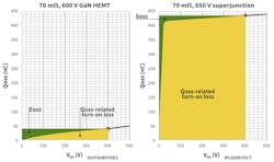
Superjunction MOSFETs are optimized for an extremely low EOSS figure of merit, which is a significant parameter loss mechanism in single-ended topologies. Conversely, GaN HEMTs have a much more favorable QOSS figure of merit. In half bridge-based circuits, the charge stored in the output capacitance and the reverse-recovery charge are more important parameters.
Figure 4 illustrates the order of magnitude reduction in losses when using GaN HEMTs. This enables ZVS with lower magnetization current and thus greatly reduced conduction losses in the switches and transformer. In addition, gate-driving losses are reduced due to the lower gate charge of GaN HEMTs.
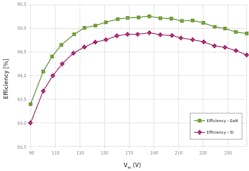
Finally, the losses associated with the charging and discharging of COSS capacitance of the switches during ZVS are also lower in GaN HEMTs than in superjunction MOSFETs. As a result, the efficiency of the entire system can be increased by around 0.4% at full load over the entire input voltage range (Fig. 5).
With order of magnitude reductions in gate charge and output charge, combined with virtually zero reverse-recovery charge, GaN-based switching devices support both simpler topologies and optimized control methods. With the bonus of improved efficiency, adapter and charger designs that replace MOSFETs with wide bandgap alternatives deliver clear benefits in competitive markets.
Gerald Deboy is Senior Principal Power Semiconductors and System Engineering, Matthias Kasper is Senior Specialist Application Engineering, Alfredo Medina Garcia is Senior Staff Engineer, and Manfred Schlenk is Senior Principal Power Systems at Infineon Technologies AG.
Reference
1. https://www.bccresearch.com/market-research/engineering/mobile-chargers-global-markets-report.html
